Power integrity (PI) ensures that all ICs on a high-speed PCB receive stable voltage across dynamic load conditions. As data rates increase and supply voltages decrease, even small impedance fluctuations in the power distribution network (PDN) can cause timing errors, jitter, and functional failures.
This article explains power integrity in high-speed PCB design, focusing on PDN behavior, decoupling strategies, plane design, and practical layout considerations.
🔗 Core topic:
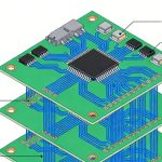
High-Speed PCB Design: Layout, Signal Integrity, Stackup, and Power Integrity
What Is Power Integrity?
Power integrity describes the ability of the PDN to deliver clean, stable power to active devices over the required frequency range.
A robust PDN must maintain low impedance from DC to high frequencies to support fast transient current demands.
Why Power Integrity Is Critical in High-Speed Designs
High-speed digital ICs exhibit:
- Fast current transients
- Low supply voltage margins
- High sensitivity to noise
Poor power integrity can result in:
- Increased jitter
- Eye diagram closure
- EMI issues
- Random system failures
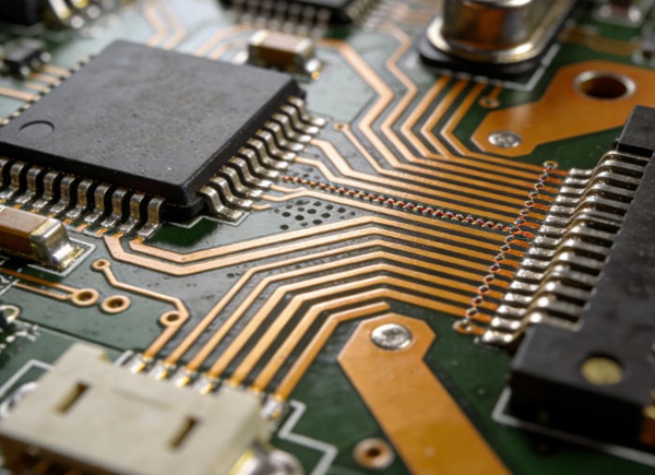
Power Distribution Network (PDN) Fundamentals
The PDN includes:
- Voltage regulators
- Power planes
- Decoupling capacitors
- IC package parasitics
Each element contributes to the overall impedance profile seen by the IC.
Target Impedance Concept
Target impedance defines the maximum allowable PDN impedance to keep voltage ripple within acceptable limits.
Key inputs include:
- Supply voltage
- Allowed ripple
- Transient current
Designing for target impedance helps guide capacitor selection and plane strategy.
Decoupling and Bypass Capacitor Strategy
Effective decoupling requires a hierarchy of capacitors:
- Bulk capacitors for low frequencies
- Ceramic capacitors for mid-to-high frequencies
- On-die or package capacitance for very high frequencies
Placement and mounting inductance are as important as capacitance value.
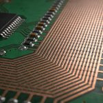
Power and Ground Plane Design
Solid power and ground planes provide:
- Low inductance current paths
- Distributed capacitance
- Improved EMI performance
Plane pair spacing and continuity directly affect PDN impedance.
🔗 Stackup dependency:
High-Speed PCB Stackup Design and Material Selection
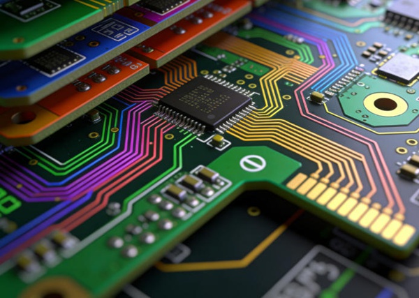
Interaction Between Power Integrity and Signal Integrity
Power noise can directly modulate signal timing and amplitude.
Common coupling mechanisms include:
- Simultaneous switching noise
- Ground bounce
- Shared return paths
PI and SI must be analyzed together in high-speed systems.
🔗 Related analysis:
Signal Integrity in High-Speed PCB Design
PDN Simulation and Measurement
PI simulation helps predict impedance profiles and resonance points.
Measurement techniques include:
- Impedance scanning
- Time-domain voltage ripple analysis
Simulation reduces guesswork and design iterations.
Manufacturing and Component Considerations
PI performance is influenced by:
- Capacitor tolerances
- Plane copper thickness
- Via quality and count
Designers should coordinate PDN requirements with fabrication capabilities.

Best Practices Summary for Power Integrity
- Define target impedance early
- Use solid planes and short return paths
- Minimize mounting inductance
- Spread capacitor values
- Validate PDN with simulation
Conclusion
Power integrity is a foundational requirement for reliable high-speed PCB operation. A well-designed PDN reduces noise, improves signal timing, and increases system robustness.
This article completes the physical-layer integrity framework for high-speed PCB design.
FAQ – Power Integrity in High-Speed PCB Design
A: Power integrity issues are caused by high PDN impedance, poor decoupling, excessive inductance, and unstable current return paths.
A: Target impedance is the maximum allowable PDN impedance that keeps voltage ripple within acceptable limits.
A: The number depends on IC requirements, PDN impedance goals, and layout quality rather than a fixed rule.
A: Yes. Power noise can cause jitter, timing errors, and false switching in high-speed signals.
A: Solid planes provide lower inductance and better high-frequency performance than wide traces.
A: While not mandatory, PDN simulation significantly reduces risk in high-speed designs.