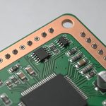
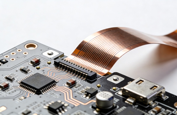
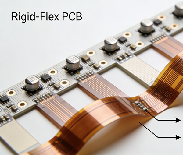
Rigid-flex PCBs combine rigid circuit boards with flexible polyimide layers into a single integrated structure. This hybrid design allows complex three-dimensional routing, reduces connectors, and improves reliability in compact electronic systems.
However, rigid-flex boards require specialized manufacturing processes that differ significantly from standard rigid PCBs. Designers must understand these processes to avoid yield issues, reliability failures, or excessive manufacturing costs.
This guide explains the rigid-flex PCB manufacturing process and the design guidelines engineers should follow to ensure reliable production.
Why Manufacturing Knowledge Matters in Rigid-Flex PCB Design
Rigid-flex PCBs are significantly more complex to manufacture than conventional rigid boards. The process involves multiple lamination cycles, selective material bonding, and precise alignment between rigid and flexible sections.
If design rules are not aligned with manufacturing capabilities, problems can occur such as:
- Delamination at rigid-flex transitions
- Cracked copper traces during bending
- Low manufacturing yield
- Increased production costs
- Reliability failures during product use
Understanding how rigid-flex boards are built allows designers to create layouts that are both manufacturable and durable.
Overview of the Rigid-Flex PCB Manufacturing Process
Rigid-flex PCB fabrication typically involves the following stages.
1. Flex Circuit Fabrication
The flexible layers are manufactured first using polyimide substrates and rolled-annealed copper.
Typical steps include:
- Polyimide material preparation
- Copper pattern imaging
- Chemical etching
- Coverlay application
- Flex circuit inspection
Rolled-annealed copper is commonly used in flex layers because it provides better fatigue resistance than electrodeposited copper.
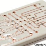
2. Rigid Layer Fabrication
Rigid PCB layers are produced similarly to standard multilayer boards.
The process includes:
- Core layer preparation
- Inner layer imaging
- Copper etching
- Lamination preparation
These layers will later be integrated with the flexible circuit layers.
3. Rigid-Flex Lamination
One of the most critical manufacturing steps is the lamination process.
The rigid layers and flex layers are bonded together using prepreg or adhesive systems through controlled heat and pressure.
Key challenges include:
- Alignment of rigid and flex sections
- Preventing resin flow into flex areas
- Maintaining dimensional stability
Improper lamination can lead to delamination or structural weakness.
4. Drilling and Via Formation
After lamination, drilling processes create vias and component holes.
Typical techniques include:
- Mechanical drilling
- Laser drilling for microvias
- Via plating
Drilling in rigid-flex boards requires careful control to avoid damaging the flexible regions.
5. Copper Plating
Copper plating strengthens vias and builds the conductive layers.
The plating process must ensure:
- Uniform copper thickness
- Reliable via connections
- Strong mechanical durability
Poor plating quality can cause open circuits or reliability failures.
6. Outer Layer Imaging and Etching
The outer copper layers are patterned using photoimaging and etching processes.
This step defines:
- signal routing
- power planes
- component pads
High precision is required because rigid-flex designs often involve dense routing.
7. Surface Finishing
Surface finishes protect copper pads and improve solderability.
Common finishes include:
- ENIG (Electroless Nickel Immersion Gold)
- Immersion Silver
- OSP (Organic Solderability Preservative)
The choice depends on assembly requirements and reliability expectations.
8. Final Profiling and Testing
The final steps include:
- board outline routing
- electrical testing
- reliability inspection
Rigid-flex boards often require additional inspection for flex reliability and lamination integrity.
Key Design Guidelines for Rigid-Flex Manufacturing
Designers should follow several important rules to ensure successful rigid-flex fabrication.
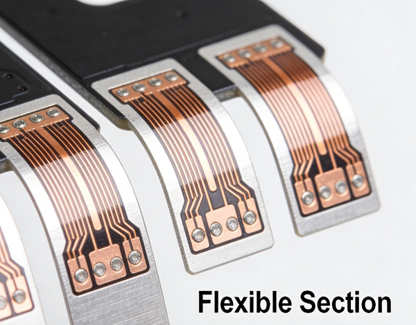
Use Gradual Rigid-to-Flex Transitions
Rigid-to-flex transition areas experience mechanical stress during bending.
Best practices include:
- avoiding sharp corners
- using curved transition shapes
- reinforcing stress areas
These design choices reduce the risk of copper cracking or delamination.
Maintain Balanced Stackups
An unbalanced stackup can cause warpage or uneven stress distribution.
Design recommendations include:
- symmetric layer structures
- uniform copper distribution
- consistent material thickness
Balanced stackups improve both manufacturability and mechanical reliability.
Avoid Vias in Flex Bend Areas
Vias introduce mechanical weaknesses in flexible sections.
Designers should:
- keep vias out of dynamic bend areas
- place vias in rigid regions whenever possible
- increase trace spacing in flex zones
This prevents fatigue failures during repeated bending.
Control Copper Thickness in Flex Layers
Thicker copper reduces flexibility and increases stress during bending.
Typical recommendations:
- 0.5 oz copper for dynamic flex
- 1 oz copper for static flex
Choosing the right copper thickness helps improve long-term durability.
Common Manufacturing Challenges in Rigid-Flex PCBs
Even well-designed boards can face production challenges if manufacturing constraints are not considered.
Typical issues include:
Delamination
Poor bonding between layers can cause rigid and flex sections to separate.
Copper Cracking
Excessive bending stress may fracture copper traces.
Registration Errors
Misalignment between layers can affect signal integrity and component placement.
Low Production Yield
Complex stackups or tight tolerances may reduce manufacturing success rates.
Collaboration between PCB designers and manufacturers is critical to avoid these problems.
Applications of Rigid-Flex PCBs
Rigid-flex technology is widely used in industries where compact design and reliability are essential.
Common applications include:
- aerospace electronics
- medical devices
- wearable technology
- military systems
- automotive electronics
- consumer electronics
These industries benefit from the space savings and durability offered by rigid-flex designs.
Conclusion
Rigid-flex PCB technology enables compact, reliable electronic systems by integrating rigid boards with flexible circuits. However, the manufacturing process is significantly more complex than standard PCB fabrication.
Designers must understand rigid-flex production techniques, including lamination, drilling, plating, and stackup control. Following proper design guidelines helps ensure high manufacturing yield and long-term product reliability.
By aligning PCB design with manufacturing capabilities, engineers can successfully implement rigid-flex technology in advanced electronic products.
FAQ: Rigid-Flex PCB Manufacturing and Design
A: Rigid-flex PCB manufacturing combines flexible circuit fabrication with traditional multilayer rigid PCB production. The typical process includes flex layer fabrication, rigid layer preparation, rigid-flex lamination, drilling and via formation, copper plating, outer layer imaging, surface finishing, and final electrical testing. Because rigid and flexible materials behave differently during lamination and drilling, the process requires specialized equipment and strict process control.
A: Rigid-flex PCBs are more expensive because they involve more complex materials and manufacturing steps. Multiple lamination cycles, specialized polyimide substrates, precision alignment, and lower production yields all contribute to higher costs. However, rigid-flex boards often reduce connectors, cables, and assembly steps, which can offset the initial PCB fabrication cost.
A: Rigid-flex PCBs typically use FR-4 materials for the rigid sections and polyimide substrates for the flexible layers. The flexible circuits usually use rolled-annealed copper, which provides better bending durability compared to electrodeposited copper. Adhesives, prepregs, and coverlays are also used to bond layers and protect flex circuits.
A: The minimum bend radius depends on the thickness and copper structure of the flex region. A common guideline is:
Static bend: 10× the flex thickness
Dynamic bend: 20× the flex thickness
Maintaining a proper bend radius prevents copper cracking and improves long-term reliability.
A: Vias should generally be avoided in dynamic flex regions because they create mechanical stress points that may lead to failures during bending. If vias must be used in flex areas, they should be placed outside the primary bend zone and designed with reinforced structures.
A: Designers can improve yield by following several best practices:
Avoid vias in bend regions
Maintain symmetric stackups
Use gradual rigid-to-flex transitions
Control copper thickness in flex layers
Work closely with PCB manufacturers during the design stage
These guidelines help reduce manufacturing defects and improve long-term product reliability.