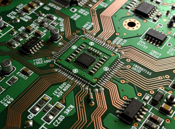
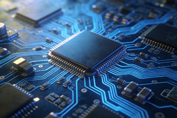
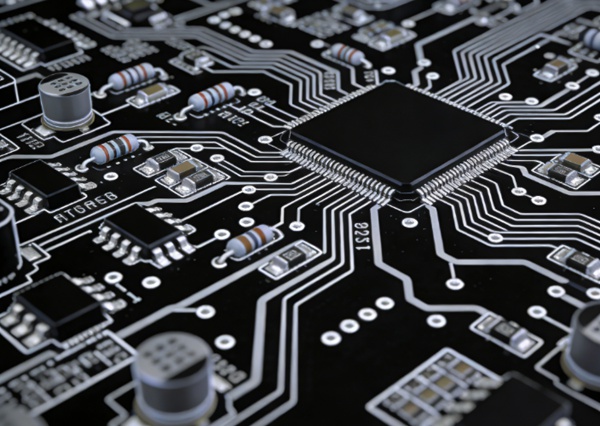
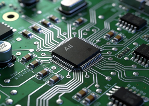
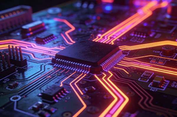
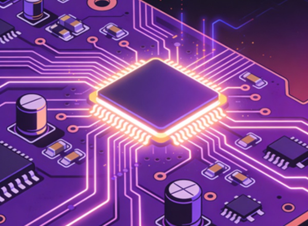
Han Sphere Blog

Explore the latest trends, technologies, and best practices in PCB design, manufacturing, and the electronics industry

The Future of AI in PCB Design Automation and Electronic Manufacturing

The Future of AI in PCB Design Automation and Electronic Manufacturing

This article explores upcoming trends in AI-powered PCB design automation. It highlights deeper EDA tool integration, real-time manufacturing feedback loops, and the consequent evolution of engineering workflows, driving greater efficiency…

Innovative PCB Design Techniques for the Future

Innovative PCB Design Techniques for the Future

Discover cutting-edge trends in PCB design shaping tomorrow's electronics. This article explores flexible and multilayer boards, advanced automated testing, and key emerging technologies. Gain expert insights to master innovative techniques…

Advanced PCB Design Tips for Enhanced Efficiency and Performance

Advanced PCB Design Tips for Enhanced Efficiency and Performance

Discover advanced PCB design tips to enhance performance and reduce errors. This guide covers signal integrity techniques, effective thermal management strategies, and essential best practices for a streamlined and successful…

PCB Design Tools: How to Choose the Right Software

PCB Design Tools: How to Choose the Right Software

Choosing the right PCB design tool is crucial for successful circuit board creation. This article covers popular tools such as KiCad, Autodesk Eagle, and Altium Designer, and offers insights into…

2025 PCB Industry Review and 2026 Outlook

2025 PCB Industry Review and 2026 Outlook

The report indicates that the PCB market experienced moderate growth in 2025, with IC substrates standing out as the brightest spot due to AI demand. For 2026, industry growth is…

About Our Blog

Han Sphere Blog shares the latest trends, technologies, and best practices in PCB design, manufacturing, and the electronics industry. Our expert team regularly shares their knowledge and experience.

Popular Posts

WhatsApp