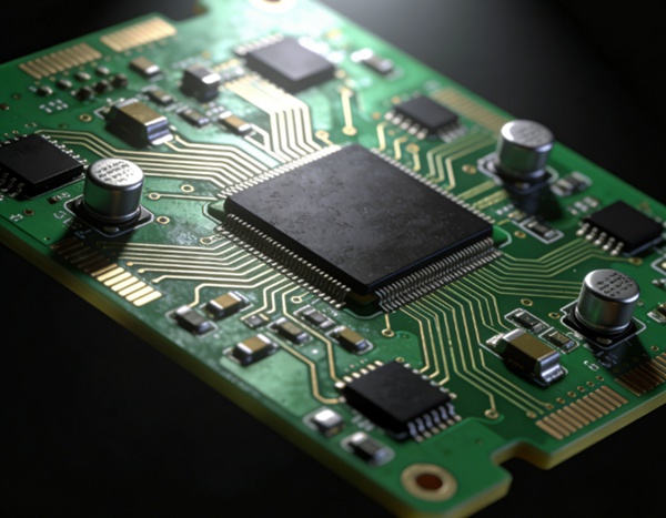
In our previous article, Mastering PCB Design, we covered the fundamental concepts of PCB design, such as component selection, the importance of a solid layout, and the general design process. However, to truly excel in PCB design, it’s essential to go beyond the basics. In this article, we will focus on advanced techniques and tips to improve your PCB design’s efficiency and performance. Whether you’re designing for high-speed applications or aiming for better thermal management, these strategies will enhance both the electrical and mechanical characteristics of your PCB.
1. Designing for High-Speed Circuits
In modern electronics, high-speed circuits are common. However, as signal frequencies increase, the design challenges also become more complex. Ensuring signal integrity is critical for high-speed performance. Below are some key strategies for successful high-speed PCB design:
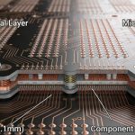
- Controlled Impedance Traces: To maintain signal integrity, make sure that the impedance of your traces is controlled. This involves matching the trace width to the layer stack-up and ensuring that signals maintain consistent impedance throughout the PCB.
- Differential Pairs: For high-speed signals, using differential pair routing can significantly improve signal quality by minimizing noise and crosstalk.
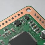
- Use of Via-Fences: Via-fences, which are ground vias placed around high-speed signals, can help shield sensitive signals from noise and reduce EMI (Electromagnetic Interference).
2. Thermal Management Strategies
Thermal issues can lead to performance degradation and even failure of your PCB components. A well-designed PCB ensures proper heat dissipation, which prolongs the life of components and enhances overall efficiency. Here are a few thermal management strategies:
- Thermal Vias: Include vias beneath heat-generating components, such as power transistors or processors, to channel heat away from these areas.
- Copper Pours for Heat Distribution: Large copper pours are often used in power circuits to spread the heat evenly across the board. This prevents localized overheating that could damage components.
- Component Placement for Heat Dissipation: Place components that generate the most heat in areas that allow airflow or direct heat dissipation. Avoid clustering heat-sensitive components near high-power components.

3. Signal Integrity and Noise Reduction
Signal integrity is crucial in PCB design, particularly when designing for high-frequency or sensitive analog circuits. Ensuring minimal noise and avoiding signal interference requires careful attention to layout. Here are some methods to reduce noise:
- Ground Planes: Implementing a solid, uninterrupted ground plane is vital to minimizing noise and ensuring a stable reference for the signals.
- Power Planes: Use dedicated power planes to distribute power more evenly, reducing the risk of voltage fluctuations that could affect the signal quality.
- Decoupling Capacitors: Place decoupling capacitors close to the power pins of ICs to stabilize voltage and reduce power noise.
- Minimize Trace Crossovers: Keep signal traces away from power traces as much as possible to reduce cross-talk and interference.
4. Design for Manufacturability (DFM)
Designing your PCB with manufacturability in mind ensures that your designs are easier to fabricate and assemble, leading to cost-effective production and fewer errors during the manufacturing process. Some DFM best practices include:
- Use Standard Components: Standardizing the components you use will help reduce costs, lead times, and minimize the risk of component shortages.
- Minimize Tight Tolerances: While precision is important, extremely tight tolerances can drive up production costs and lead to potential fabrication issues. Strive for reasonable tolerances that balance precision with cost-effectiveness.
- Panelization: Design your PCB to fit within standard panel sizes used by manufacturers to minimize wasted material during the production process.
5. Reducing EMI (Electromagnetic Interference)
As electronics get more compact, the risk of EMI increases. EMI can cause malfunctioning of sensitive circuits, particularly in high-frequency and analog designs. Here are some ways to reduce EMI in your PCB design:
- Shielding: Implement shielding in critical areas to prevent electromagnetic radiation from escaping or entering sensitive circuits. Use copper pours or external shielding cans where appropriate.
- Via Fencing: Surround sensitive traces with ground vias to create a barrier that shields against noise and EMI.
- Use Proper Trace Routing: Keep high-frequency traces away from noisy areas, and ensure they follow controlled impedance paths.
Conclusion
Designing high-performance PCBs requires a deep understanding of not only basic PCB design principles but also advanced techniques like thermal management, signal integrity, noise reduction, and manufacturability. By incorporating these advanced tips into your workflow, you can create more reliable, efficient, and cost-effective PCBs. Whether you’re designing for high-speed circuits or managing thermal issues, these strategies will ensure your PCB designs are optimized for performance.
For more in-depth insights into PCB design, check out our previous post on Mastering PCB Design, where we discuss foundational principles, tools, and strategies for beginners and professionals alike.
Related Articles:
PCB Design FAQs
A: Controlled impedance refers to maintaining a consistent impedance in the traces of a PCB. It is crucial for high-speed signal integrity, as it minimizes reflection, ensures proper signal transmission, and avoids loss.
A: You can manage heat in PCB design by using thermal vias to conduct heat away from hot components, placing copper pours for heat distribution, and ensuring components are spaced for better airflow. Heat sinks may also be added for high-power components.
A: Ground planes provide a continuous reference for signals and offer a low-impedance path for the return currents. A solid ground plane reduces noise and minimizes electromagnetic interference (EMI).
A: Improving manufacturability involves using standard components, minimizing tight tolerances, designing for panelization, and checking that your design meets fabrication capabilities. This helps reduce production errors and costs.
A: Via fences are groups of ground vias placed around sensitive traces to act as a barrier to electromagnetic interference (EMI). They help shield high-speed signals and minimize cross-talk and external noise.