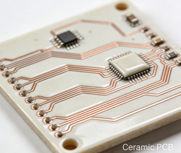
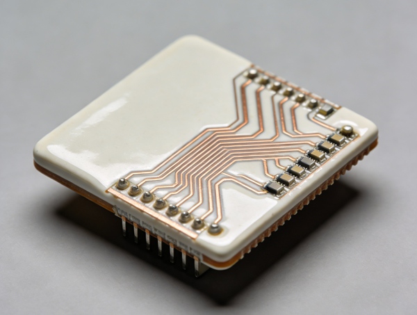
Ceramic circuit boards are used in applications where conventional FR4 boards cannot provide sufficient thermal performance or temperature stability. Power electronics, LED modules, and RF systems often require substrates capable of handling high heat loads and harsh operating conditions.
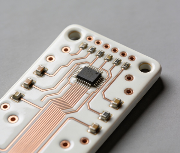
Unlike standard PCBs that use fiberglass laminates, ceramic boards use materials such as alumina or aluminum nitride as the substrate. These materials provide much higher thermal conductivity and excellent electrical insulation.
For a broader overview of ceramic substrate design considerations, see Ceramic PCB Design Guide.
Because ceramic materials behave differently from fiberglass laminates, they require specialized manufacturing processes. The most common technologies include Direct Bonded Copper (DBC), Direct Plated Copper (DPC), and Thick Film circuits.
Overview of Ceramic PCB Manufacturing Technologies
The choice of manufacturing technology depends on several design requirements, including:
- required copper thickness
- circuit density
- thermal performance
- production cost
Each process has unique advantages and limitations.
Direct Bonded Copper (DBC)
Direct Bonded Copper is one of the most widely used processes for ceramic power modules.
In this process, a thick copper foil is bonded directly to the ceramic substrate at high temperature. The bonding occurs through a controlled oxidation process that forms a strong metallurgical bond between the copper and the ceramic surface.
Typical process steps include:
- ceramic substrate preparation
- copper foil placement
- high-temperature bonding process
- circuit pattern etching
- surface finishing
DBC boards usually use alumina or aluminum nitride substrates.
Because the copper layer is relatively thick, DBC boards can handle high current and provide excellent heat spreading. For this reason, they are commonly used in power electronics such as IGBT modules and automotive inverters.
Thermal considerations for these applications are discussed in Thermal Management in PCB Design.
Direct Plated Copper (DPC)
Direct Plated Copper technology uses electroplating instead of copper foil bonding.
In this process, a thin metal seed layer is first deposited on the ceramic surface. Copper is then plated directly onto the substrate to form the circuit pattern.
Typical process flow includes:
- substrate surface treatment
- thin metal seed layer deposition
- photolithography patterning
- copper electroplating
- circuit finishing
Because copper is deposited through plating, DPC allows much finer line widths compared with DBC.
This makes DPC suitable for:
- high-density LED modules
- RF circuits
- sensor modules
The ability to produce fine traces also supports high-frequency circuit design. More details can be found in High-Frequency PCB Design Guide.
Thick Film Technology
Thick film circuits are manufactured using a printing process rather than traditional PCB etching.
A conductive paste, usually containing silver or gold particles, is screen-printed onto the ceramic substrate. The board is then fired at high temperature to sinter the conductive material and form the circuit.
Typical steps include:
- conductive paste preparation
- screen printing pattern
- high-temperature firing
- optional multilayer printing
Thick film circuits have been used for many years in hybrid microelectronics.
Although this process does not support extremely fine traces, it offers several advantages:
- relatively low production cost
- good reliability in harsh environments
- compatibility with multilayer ceramic circuits
Because of these properties, thick film circuits are often used in sensors, automotive electronics, and industrial control systems.
Reliability considerations for such environments are discussed in PCB Failure Analysis Guide.
Comparison of Ceramic PCB Manufacturing Methods
The following table summarizes key differences between the three manufacturing processes.
| Technology | Key Advantage | Typical Copper Thickness | Applications |
|---|---|---|---|
| DBC | excellent thermal performance | thick copper | power modules |
| DPC | fine trace capability | thin to medium copper | LED and RF circuits |
| Thick Film | lower cost process | printed conductive paste | hybrid circuits |
Engineers should select the manufacturing technology based on electrical performance, thermal requirements, and circuit density.
Manufacturing Challenges for Ceramic PCBs
Although ceramic PCBs provide significant performance advantages, they also introduce several manufacturing challenges.
Ceramic materials are brittle and must be handled carefully during processing. In addition, thermal expansion differences between copper and ceramic substrates can introduce mechanical stress.
Specialized fabrication equipment and process control are often required to ensure reliable bonding between the copper layers and the ceramic material.
More details about cost and design considerations can be found in Ceramic PCB Cost Factors.
Conclusion
Ceramic PCBs use several specialized manufacturing technologies that differ from traditional FR4 fabrication.
Direct Bonded Copper provides excellent thermal performance for high-power electronics. Direct Plated Copper supports fine circuit patterns for RF and LED applications. Thick film technology offers a simpler and often lower-cost solution for hybrid circuits.
Selecting the appropriate manufacturing process depends on the electrical, thermal, and mechanical requirements of the final product.
For designers working with ceramic substrates, understanding these fabrication methods is an important step in achieving reliable circuit performance.
Ceramic PCB Manufacturing Process FAQ
A: Direct Bonded Copper (DBC) is widely used in power electronics because it provides thick copper layers and excellent thermal conductivity.
A: DBC bonds copper foil directly to the ceramic substrate, while DPC uses electroplating to deposit copper onto the ceramic surface.
A: Ceramic materials have different thermal and mechanical properties than fiberglass laminates, so specialized bonding and metallization processes are required.
A: DPC technology allows finer trace widths, making it suitable for high-density LED modules and RF circuits.
A: Yes. Thick film technology is still widely used in hybrid circuits, sensors, and industrial electronics where reliability and environmental stability are important.