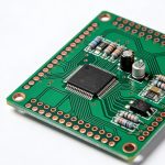
The Rigid Printed Circuit Board (Rigid PCB) remains the workhorse of the electronics industry. While flexible and HDI boards grab the headlines, the reliability and cost-effectiveness of a standard rigid board are what power 90% of industrial, automotive, and consumer devices.
However, “simple” doesn’t mean “easy.” A high-quality Rigid PCB requires a deep understanding of material science and Design for Manufacturing (DFM). At Hansphere, we believe every great product starts with a flawless rigid foundation.
1. Material Selection: Beyond Standard FR-4
Most rigid boards use FR-4 (Flame Retardant 4), a glass-reinforced epoxy laminate. But not all FR-4 is created equal.
- Tg (Glass Transition Temperature): For high-reliability or lead-free soldering, you must choose High-Tg FR-4 (over $170$°C) to prevent board warping and barrel cracking in vias.
- CTI (Comparative Tracking Index): Crucial for high-voltage applications to prevent electrical breakdown across the board surface.
- Pro Tip: If your design involves high-power LEDs or power converters, consider an Aluminum-clad Rigid PCB or Ceramic PCB for superior thermal dissipation.
What Is a Rigid PCB?
A rigid PCB is a circuit board made from solid, non-flexible substrate materials—typically FR-4—that maintains its shape throughout operation.
Key characteristics:
- Mechanical rigidity
- Multilayer support
- Mature manufacturing ecosystem
- Cost-effective at scale
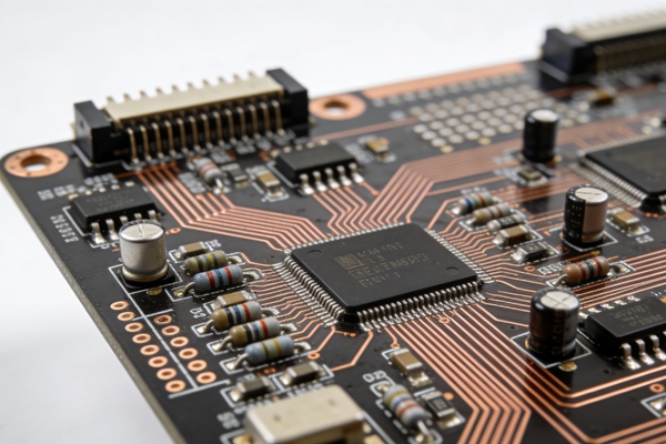
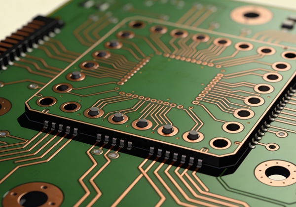
2. The Anatomy of a Rigid PCB Layout
Layer Stack-up and Symmetry
A balanced stack-up is essential to prevent “Potato Chipping” (bowing and twisting) during the reflow process.
- The Symmetry Rule: Your copper distribution and dielectric thickness must be symmetrical around the center of the board’s Z-axis.
- Expert Insight: For a standard 4-layer board, a
Signal-Ground-Power-Signalstack-up provides the best balance of EMI shielding and routing space.
Trace Width and Copper Weight
- Current Capacity: Don’t guess your trace widths. Use the IPC-2152 standard to calculate the required width based on your current and allowable temperature rise.
- Standard Copper: Most PCB Manufacturing defaults to 1oz ($35\mu m$) copper. For high-current industrial boards, you may need Heavy Copper (2oz or 3oz).
Rigid PCB vs Other PCB Types
| PCB Type | Key Difference |
|---|---|
| HDI PCB | Higher density, higher cost |
| Flexible PCB | Bendable, higher material cost |
| Rigid-Flex PCB | Combines both, complex fabrication |
5 Steps to a Manufacturable Rigid PCB Design
Target: Junior Engineers & PCB Layout Designers
Goal: Reducing Revision Cycles and Manufacturing Costs
- Step 1: Set Up Your Design Rules (DRC)
Before placing a single component, input your manufacturer’s capabilities into your PCB Design Tools.
Min Trace/Space: e.g., 4/4 mil (0.1/0.1mm).
Min Hole Size: e.g., 0.2mm. - Step 2: Strategic Component Placement
Group functional blocks together (e.g., Power, Analog, Digital). Keep connectors on the board edge for easier PCB Assembly and user access.
- Step 3: Ground Plane Strategy
In modern High-Speed PCB Design, a solid ground plane is your best friend. It provides a low-impedance return path and minimizes noise.
- Step 4: Choose the Right Surface Finish
HASL: Cost-effective, but not ideal for fine-pitch BGA.
ENIG (Electroless Nickel Immersion Gold): The gold standard for flat pads and long shelf life.
OSP: Great for high-volume, cost-sensitive consumer electronics. - Step 5: Generate the Fabrication Package
Export your Gerber X2 or ODB++ files along with a clear Fab Drawing that specifies board thickness, solder mask color, and any special tolerances.
3. Common Design Pitfalls to Avoid
- Acid Traps: Avoid acute angles (less than 90 degrees) in your traces. These can trap etching chemicals and “over-etch” the copper, leading to open circuits.
- Missing Solder Mask Dams: Ensure there is enough solder mask between pads to prevent solder bridging during PCB Assembly.
- Inadequate Clearance: Don’t run traces too close to the board edge. Friction during routing or V-scoring can expose the copper.
4. Advancing Beyond the Basics
Once you master rigid fundamentals, you can explore higher-density technologies:
Rigid-Flex PCB: Integrating rigid sections with flexible interconnects for 3D packaging.
HDI-PCB: Using blind and buried vias to save space.
FAQ – Rigid PCB Design Fundamentals
A: The industry standard is 1.6mm (0.062″), but at Hansphere, we can manufacture boards ranging from 0.4mm to 6.0mm depending on your mechanical requirements.
A: If your design has complex ICs or requires EMI compliance, a 4-layer board with dedicated ground and power planes is highly recommended. It offers much better signal integrity than a 2-layer design.
A: Absolutely. Every order at Hansphere undergoes a professional DFM (Design for Manufacturing) review to catch errors before they become expensive mistakes.
Conclusion
A successful Rigid PCB design is a combination of electrical logic and mechanical common sense. By following IPC standards and maintaining a strong dialogue with your manufacturer, you can ensure your project is delivered on time, on budget, and ready for the real world.
Ready to start your next project? Whether it’s a simple prototype or a massive production run, Hansphere’s Technical Team is here to help. Get a Quote Now and experience the Hansphere difference.