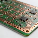
Electromagnetic interference (EMI) and electromagnetic compatibility (EMC) are critical challenges in high-speed PCB design. As edge rates increase and board density rises, PCBs become efficient sources and victims of electromagnetic noise.
This article explains EMI and EMC considerations in high-speed PCB design, focusing on root causes, coupling mechanisms, and practical mitigation strategies at the layout, stackup, and system levels.
🔗 Part of the core series:
High-Speed PCB Design: Signal Integrity, Power Integrity, and EMI Control
Understanding EMI and EMC in High-Speed PCBs
- EMI refers to unwanted electromagnetic emissions generated by a PCB
- EMC refers to the PCB’s ability to operate correctly in its electromagnetic environment
High-speed PCBs must both limit emissions and maintain immunity.
Why High-Speed Designs Are Prone to EMI
High-speed PCBs inherently increase EMI risk due to:
- Fast rise and fall times
- High-frequency harmonics
- Dense routing and tight spacing
- Discontinuous return paths
EMI is more strongly correlated with edge rate than clock frequency.
Common EMI Sources in High-Speed PCB Design
Signal Traces and Interconnects
High-speed signal traces act as antennas when:
- Return paths are broken
- Trace lengths approach resonant dimensions
- Impedance discontinuities exist
Power Distribution Networks
Poor power integrity creates voltage ripple and ground bounce, which can radiate as EMI.
🔗 Related topic:
Power Integrity in High-Speed PCB Design
Cables, Connectors, and I/O Interfaces
External interfaces often dominate EMI test failures due to common-mode currents.
EMI Coupling Mechanisms
Understanding coupling mechanisms is essential for mitigation.
Conducted Coupling
Noise travels through power or signal conductors.
Capacitive Coupling
Electric fields couple noise between adjacent structures.
Inductive Coupling
Magnetic fields induce noise in nearby loops.
Radiated Coupling
Structures radiate electromagnetic energy into free space.
Stackup and Plane Design for EMI Control
Stackup decisions directly affect EMI performance.
Best practices include:
- Solid, continuous reference planes
- Tight plane-to-plane spacing
- Dedicated ground planes for high-speed layers
🔗 Stackup dependency:
High-Speed PCB Stackup Design and Material Selection
Layout Techniques to Reduce EMI
Effective EMI reduction starts at the layout stage.
Key techniques:
- Minimize loop area
- Route high-speed signals close to reference planes
- Avoid routing across plane splits
- Shorten return current paths
🔗 Layout fundamentals:
High-Speed PCB Layout and Routing Best Practices
Controlling EMI at the Source
Source suppression is more effective than filtering later.
Methods include:
- Slowing edge rates where possible
- Proper termination
- Reducing simultaneous switching noise
- Controlling impedance discontinuities
Filtering, Shielding, and Grounding Strategies
When layout alone is insufficient:
- Use common-mode chokes on I/O
- Apply ferrite beads selectively
- Implement shielding at enclosure or PCB level
- Design grounding with controlled current paths
These should complement—not replace—good PCB design practices.
EMI Testing and Compliance Considerations
EMI compliance testing is typically performed late in development, making early design discipline critical.
Designers should:
- Anticipate regulatory requirements
- Design margin into EMI performance
- Use pre-compliance testing when possible
Best Practices Summary for EMI/EMC Control
- Control edge rates and impedance
- Maintain continuous return paths
- Use solid planes and symmetric stackups
- Minimize loop areas
- Address EMI at the source
Conclusion
EMI and EMC challenges are an inevitable part of high-speed PCB design. By understanding coupling mechanisms and applying disciplined layout, stackup, and power design strategies, engineers can significantly reduce EMI risk and improve system robustness.
This article completes the electrical integrity framework for high-speed PCB design.
FAQ – EMI and EMC in High-Speed PCB Design
A: EMI is caused by fast edge rates, large current loops, impedance discontinuities, and poor return path control.
A: EMI is primarily a layout and stackup problem; components usually play a secondary role.
A: Yes. Slower edge rates reduce high-frequency harmonics and radiated emissions.
A: Poor power integrity increases ground bounce and voltage noise, which can radiate as EMI.
A: Continuous ground planes are one of the most effective tools for EMI reduction in high-speed PCBs.
A: Some issues can be mitigated, but most effective EMI control must be designed in from the beginning.