HDI PCB technology enables high-density and high-performance electronic designs, but it also introduces unique failure mechanisms not commonly seen in standard PCBs. Understanding these failure modes is critical for improving reliability and preventing costly field failures.
This article covers HDI PCB failure analysis and reliability risks, providing engineers with practical insight into root causes, detection methods, and prevention strategies.
🔗 Part of the HDI PCB Design Series
HDI PCB Design: Technology, Stackup, Routing, and Manufacturing
Why HDI PCBs Fail Differently
HDI PCBs are more sensitive due to:
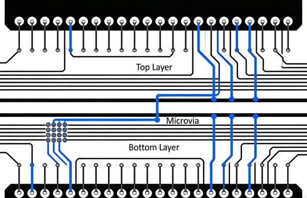
- Microvia structures
- Multiple lamination interfaces
- Thin dielectric layers
- Fine-line conductors
These factors amplify the impact of design and process variations.
Common HDI PCB Failure Modes
Microvia Cracking
Caused by:
- Thermal cycling
- Poor via filling
- CTE mismatch
Microvia cracking often leads to intermittent failures.
Interfacial Delamination
Occurs at:
- Lamination interfaces
- Copper–resin boundaries
Triggered by thermal stress and poor material compatibility.
Plating Voids and Incomplete Fill
Results from:
- Inadequate via filling
- Poor plating control
These defects compromise mechanical and electrical reliability.
Trace Over-Etching and Opens
Fine lines increase susceptibility to:
- Over-etching
- Process drift
This leads to open circuits under thermal or mechanical stress.
Failure Analysis Techniques for HDI PCBs
Cross-Section Analysis
- Reveals microvia and lamination defects
- Essential for root cause identification
X-Ray Inspection
- Detects voids and misalignment
- Non-destructive
Thermal Cycling Tests
- Simulates operating stress
- Exposes fatigue-related failures
Design-Related Reliability Risks
Poor reliability often originates from:
- Excessive stacked microvias
- Aggressive minimum rules
- Inadequate power/ground structures
🔗 Design influence:
HDI PCB Routing Rules and BGA Fanout Techniques
Manufacturing-Related Reliability Risks
Common manufacturing contributors:
- Process variability
- Insufficient inspection
- Unvalidated materials
🔗 Manufacturing impact:
HDI PCB Manufacturing Process and Yield Optimization

Preventive Design Strategies
To reduce HDI failures:
- Limit stacked microvias
- Use proven materials
- Design conservatively where possible
- Validate with pilot builds
Reliability Testing and Qualification
Recommended tests include:
- Thermal cycling
- Mechanical stress tests
- Environmental exposure
Testing should reflect real-world conditions.
Best Practices Summary
- Understand HDI-specific failure mechanisms
- Address reliability during design—not after
- Collaborate closely with manufacturers
- Verify designs with robust testing
Conclusion
HDI PCB reliability depends on a deep understanding of failure mechanisms and disciplined design and manufacturing practices. By proactively addressing reliability risks, engineers can fully realize the benefits of HDI technology while minimizing field failures.
This article completes the HDI PCB Design content cluster with a strong emphasis on real-world reliability.
FAQ – HDI PCB Failure Analysis
A: Microvia cracking caused by thermal stress.
A: Not inherently; reliability depends on design and process quality.
A: Often no; X-ray or cross-section analysis is required.
A: By using conservative rules and validated materials.
A: Yes, especially without strict process control.
A: Before volume production, during pilot builds.