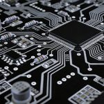
High-speed PCB designs that perform well electrically can still fail during fabrication or assembly if manufacturing constraints are not considered early. As layer counts increase, materials become more specialized, and tolerances tighten, manufacturability and yield become critical success factors.
This article explains how to design high-speed PCBs for manufacturing and yield, focusing on stackup feasibility, impedance tolerance, process variation, and collaboration with PCB fabricators.
Part of the core series:
High-Speed PCB Design: Layout, Signal Integrity, Power Integrity, EMI, and Manufacturing

Why Manufacturability Matters in High-Speed PCB Design
High-speed PCBs amplify small variations:
- Trace width deviations affect impedance
- Dielectric thickness variation impacts delay and loss
- Via quality influences signal and power integrity
Poor manufacturability leads to:
- Low yield
- Inconsistent electrical performance
- Increased cost and lead time
Designing for yield is as important as designing for performance.
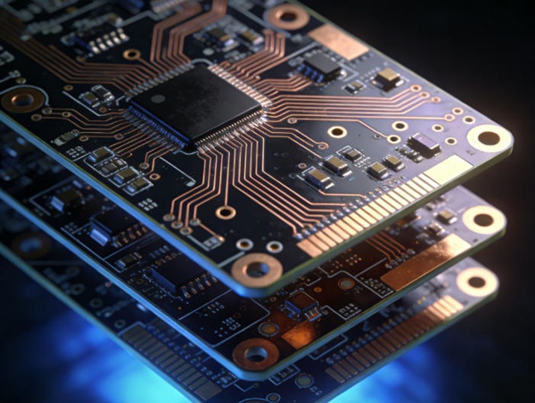
Stackup Feasibility and Fabrication Tolerances
Stackup design must align with real fabrication capabilities.
Key considerations:
- Dielectric thickness availability
- Copper weight control
- Symmetry for lamination stability
- Registration tolerance between layers
🔗 Stackup fundamentals:
High-Speed PCB Stackup Design and Material Selection
Fabricators should review stackups before layout begins.
Controlled Impedance and Yield Risk
Controlled impedance routing introduces yield sensitivity.
Best practices include:
- Avoiding extreme trace widths
- Allowing reasonable impedance tolerance
- Using consistent geometries across layers
- Defining impedance test structures
Tighter impedance targets increase cost and scrap risk.
Via Design and Drill Reliability
Vias are a major yield driver in high-speed PCBs.
Risk factors include:
- High aspect ratios
- Small finished hole sizes
- Back-drilled vias
- Dense via arrays
Designing vias within standard fabrication limits improves reliability.
Material Selection and Supply Chain Considerations
Advanced laminates improve electrical performance but may:
- Increase lead time
- Limit fabricator options
- Raise cost variability
Material choices should balance electrical needs with availability and process maturity.
🔗 Electrical dependency:
Signal Integrity in High-Speed PCB Design
Solder Mask, Surface Finish, and Assembly Yield
Assembly choices influence final yield.
Key factors:
- Solder mask registration accuracy
- Surface finish compatibility
- Pad design for fine-pitch components
High-speed designs often require tighter assembly process control.
Design for Test and Inspection
High-speed PCBs should include provisions for:
- Impedance coupons
- Electrical test access
- Inspection fiducials
Testing capability improves early defect detection and yield learning.
Collaboration with PCB Manufacturers
Early communication with fabricators enables:
- Stackup optimization
- Realistic impedance targets
- Risk identification before layout
DFM reviews should be integrated into the design workflow.
Best Practices Summary for Manufacturing and Yield
- Validate stackup feasibility early
- Balance impedance control with tolerance
- Design vias conservatively
- Choose materials with stable supply
- Include test structures
- Engage fabricators early
Conclusion
High-speed PCB success depends not only on electrical design but also on manufacturability and yield. By designing within proven fabrication limits and collaborating closely with manufacturers, engineers can achieve consistent performance, predictable cost, and scalable production.
This article completes the end-to-end high-speed PCB design framework, from signal behavior to mass production.
FAQ – High-Speed PCB Manufacturing and Yield
A: Tighter tolerances, advanced materials, and complex stackups increase sensitivity to process variation.
A: Only as tight as required. Overly strict tolerances increase cost and scrap without improving performance.
A: No. They should be used only when stub effects significantly impact signal integrity.
A: Yes. Variations in trace width, dielectric thickness, and via quality directly affect SI and PI.
A: Yes. Early review reduces redesign risk and improves yield predictability.
A: By aligning design rules with fabrication capabilities and including test structures.