A structured design review is one of the most effective ways to prevent costly re-spins in high-speed PCB projects. Many failures related to signal integrity, power integrity, EMI, or manufacturing yield can be identified early by applying a disciplined checklist.
This High-Speed PCB Design Review Checklist provides a comprehensive, experience-based framework to review high-speed PCB designs before fabrication.
1. System & Architecture Review
- ⬜ High-speed interfaces clearly identified
- ⬜ Data rates and edge rates defined
- ⬜ Timing margins documented
- ⬜ Power domains and voltage tolerances defined
- ⬜ Environmental conditions considered (temperature, noise)
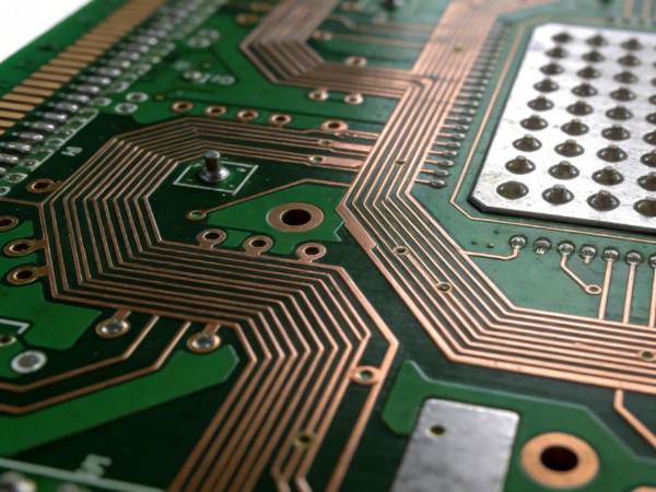
2. Stackup & Material Review
- ⬜ Stackup reviewed and approved by PCB fabricator
- ⬜ Symmetric stackup structure used
- ⬜ High-speed signal layers adjacent to solid reference planes
- ⬜ Dielectric thickness supports target impedance
- ⬜ Material Dk and Df appropriate for data rate
- ⬜ Glass weave effects considered for differential pairs
🔗 Reference:
High-Speed PCB Stackup Design and Material Selection
3. Impedance & Transmission Line Review
- ⬜ Target impedance defined for all high-speed nets
- ⬜ Trace width and spacing within fabrication tolerance
- ⬜ Impedance controlled consistently across layers
- ⬜ Minimal impedance discontinuities
- ⬜ Test coupons defined if required
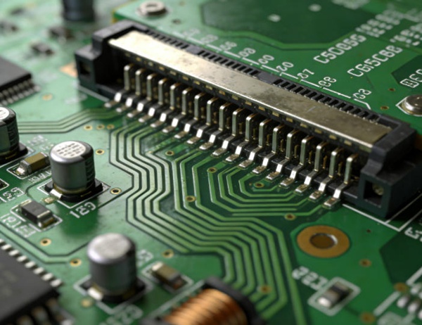
4. High-Speed Layout & Routing Review
- ⬜ Critical nets routed first
- ⬜ High-speed traces routed close to reference planes
- ⬜ No routing across plane splits
- ⬜ Differential pairs length-matched and symmetry maintained
- ⬜ Parallel routing minimized to reduce crosstalk
- ⬜ Via count minimized on critical nets
🔗 Reference:
High-Speed PCB Layout and Routing Best Practices
5. Return Path & Reference Plane Review
- ⬜ Continuous return paths for all high-speed signals
- ⬜ Reference plane transitions managed with stitching vias
- ⬜ No broken return paths under critical signals
- ⬜ Ground plane integrity maintained
6. Signal Integrity Review
- ⬜ SI risks identified early
- ⬜ Reflections controlled with termination where needed
- ⬜ Crosstalk within acceptable limits
- ⬜ Via stubs evaluated and mitigated if required
- ⬜ Simulation results reviewed (if applicable)
🔗 Reference:
Signal Integrity in High-Speed PCB Design
7. Power Integrity Review
- ⬜ Target impedance defined for each power rail
- ⬜ Adequate decoupling hierarchy implemented
- ⬜ Capacitors placed close to IC power pins
- ⬜ Low-inductance power and ground planes used
- ⬜ PDN resonance risks evaluated
🔗 Reference:
Power Integrity in High-Speed PCB Design
8. EMI / EMC Review
- ⬜ Loop areas minimized
- ⬜ Edge rates controlled where possible
- ⬜ Solid ground planes used for shielding
- ⬜ I/O interfaces reviewed for EMI risk
- ⬜ EMI mitigation planned at the source
🔗 Reference:
EMI and EMC Considerations in High-Speed PCB Design
9. Manufacturing & Yield Review
- ⬜ Stackup compatible with fabrication capabilities
- ⬜ Controlled impedance tolerance realistic
- ⬜ Via sizes and aspect ratios manufacturable
- ⬜ Advanced materials available and qualified
- ⬜ Assembly constraints reviewed
🔗 Reference:
High-Speed PCB Design for Manufacturing and Yield
10. Testability & Validation Review
- ⬜ Impedance and electrical test structures included
- ⬜ Probe access for critical signals
- ⬜ Power rail measurement points provided
- ⬜ Debug strategy defined
Final Review Gate
- ⬜ All checklist items reviewed and approved
- ⬜ Risks documented with mitigation plans
- ⬜ Design frozen for fabrication
Conclusion
A disciplined design review process significantly reduces the risk of high-speed PCB failures. This checklist consolidates best practices across signal integrity, power integrity, EMI, stackup design, and manufacturing to support reliable, scalable high-speed systems.
This checklist serves as a practical engineering reference for both design teams and reviewers.
FAQ – High-Speed PCB Design Review
A: Before layout completion and again before release to fabrication.
A: Yes. It applies broadly to DDR, PCIe, USB, Ethernet, and similar interfaces.
A: No. It complements simulation by catching structural and process-related risks.
A: Designers, SI/PI engineers, manufacturing partners, and test engineers.
A: Yes. It should be adapted based on project complexity and risk level.