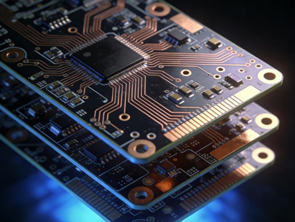
Stackup design and material selection form the physical foundation of high-speed PCB performance. Even with perfect routing and signal integrity analysis, an improper stackup or unsuitable laminate can introduce impedance variation, excessive loss, and manufacturing risk.
This article explains how to design an effective high-speed PCB stackup and select appropriate materials, focusing on electrical performance, manufacturability, and cost balance.
🔗 Core topic:
High-Speed PCB Design: Layout, Signal Integrity, and Stackup Fundamentals
Why Stackup Design Matters in High-Speed PCBs
In high-speed designs, traces no longer behave as simple conductors. The electromagnetic field around each signal interacts directly with the surrounding dielectric and reference planes.
Stackup design determines:
- Characteristic impedance
- Signal loss and dispersion
- Return path quality
- Crosstalk behavior
- EMI performance
A well-designed stackup reduces the need for layout compromises later.
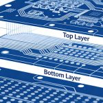
Typical High-Speed PCB Stackup Structures
Symmetric Stackup Philosophy
High-speed PCBs generally use symmetric stackups to ensure:
- Mechanical stability
- Uniform impedance control
- Reduced warpage during fabrication
Symmetry also simplifies manufacturing and improves yield.
Common Layer Configurations
Typical high-speed stackups include:
- 4-layer: Entry-level high-speed designs
- 6–8 layer: Most mainstream high-speed digital boards
- 10+ layer: Dense, multi-interface systems
Critical signals are usually routed adjacent to solid reference planes.
Dielectric Material Properties That Affect High-Speed Signals
Dielectric Constant (Dk)
Dk determines signal propagation speed and impedance. Lower and more stable Dk values are preferred for high-speed designs.
Material consistency across frequency and temperature is often more important than absolute Dk value.
Dissipation Factor (Df)
Df represents dielectric loss and directly affects signal attenuation.
For high-speed interfaces, especially long channels, low Df materials help preserve eye openings and timing margins.
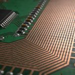
Glass Weave Effects
Glass weave patterns can introduce impedance variation and skew, especially for differential pairs.
Mitigation strategies include:
- Spread-glass materials
- Routing at angles to the weave
- Tight impedance control
FR-4 vs High-Speed Laminates
Standard FR-4 materials are sufficient for many designs, but limitations appear at higher data rates.
High-speed laminates offer:
- Lower Df
- More stable Dk
- Improved signal integrity
Material choice should be based on performance requirements rather than default assumptions.
Stackup Design for Impedance Control
Impedance control begins at the stackup level.
Best practices include:
- Defining target impedance early
- Selecting dielectric thickness based on routing constraints
- Keeping signal layers close to reference planes
- Avoiding unnecessary layer transitions
Impedance should be validated with fabrication partners.
🔗 Routing dependency:
High-Speed PCB Layout and Routing Best Practices
Return Path Planning in Stackup Design
Continuous return paths depend on proper plane placement.
Key considerations:
- Dedicated reference planes for high-speed layers
- Minimizing plane splits
- Coordinating signal transitions with reference plane changes
Stackup decisions strongly influence return current behavior.
🔗 SI relationship:
Signal Integrity in High-Speed PCB Design
Manufacturing and Cost Considerations
Advanced materials and complex stackups increase fabrication cost.
Designers should balance:
- Electrical performance
- Material availability
- Fabrication yield
- Total system cost
Early collaboration with PCB manufacturers reduces risk and iteration cycles.
Best Practices Summary for High-Speed PCB Stackup Design
- Use symmetric stackups
- Place high-speed signals adjacent to solid planes
- Select materials based on loss and stability
- Plan impedance at the stackup stage
- Align electrical goals with manufacturing constraints
Conclusion
Stackup design and material selection are foundational to successful high-speed PCB design. A disciplined approach at this stage enables cleaner routing, stronger signal integrity, and predictable manufacturing outcomes.
This article completes the core technical framework for high-speed PCB physical design.
FAQ – High-Speed PCB Stackup and Materials
A: The required layer count depends on routing density, impedance requirements, and power distribution needs.
A: FR-4 can support many high-speed designs, but higher data rates may require low-loss laminates.
A: Symmetric stackups improve mechanical stability and manufacturing reliability.
A: Higher Df increases signal loss, reducing eye opening and timing margin.
A: Yes. Proper plane placement and return path control significantly reduce EMI risk.
A: Material decisions should be made early, ideally before detailed routing begins.