In the ever-evolving world of PCB design, staying ahead of technological advancements is critical for ensuring that your designs meet future demands. In our previous article, Advanced PCB Design Tips for Enhanced Efficiency and Performance, we explored techniques to improve signal integrity, thermal management, and manufacturability. Now, let’s dive into some of the most innovative techniques and emerging trends in PCB design that will shape the future of electronics.
From flexible PCBs to multilayer designs and automated testing, these technologies are becoming increasingly vital for creating smaller, faster, and more reliable devices.
1. Flexible PCBs: Enabling the Next Generation of Wearable and Portable Devices
Flexible PCBs (FPCBs) are revolutionizing the design of electronics, particularly for wearable technology, medical devices, and compact electronics. Unlike traditional rigid PCBs, flexible circuits can bend, fold, and twist without damaging the components, making them ideal for applications where space is limited and flexibility is needed.
1.1 Advantages of Flexible PCBs
- Space Optimization: Flexible PCBs can be integrated into non-traditional shapes and sizes, allowing for more compact designs. They are ideal for wearable devices, medical implants, and even in automotive applications where space constraints are significant.
- Durability: Flexible PCBs are typically more resistant to shock and vibration, making them perfect for devices subject to movement or environmental stress, such as smartphones and fitness trackers.
- Lightweight and Thin Designs: Flexible PCBs enable the design of thinner and lighter devices, which is particularly important in industries like consumer electronics and healthcare.
1.2 Design Challenges with Flexible PCBs
While flexible PCBs offer many advantages, they also present unique challenges. For instance, their mechanical properties require specialized handling during manufacturing, and the materials used must be carefully chosen to balance flexibility with durability. Key considerations include:
- Material Selection: Flex circuits require materials that are both conductive and flexible. Polyimide is one of the most commonly used materials for flexible PCBs due to its excellent mechanical strength and high thermal stability.
- Bend Radius: Designers must ensure that the PCB design accounts for the bend radius, as excessive bending can damage the traces. The bend radius should be large enough to prevent stress on the circuit, which could lead to failure.
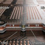
2. Multilayer PCB Design: Improving Density and Performance
Multilayer PCBs are commonly used when designing high-density circuits. These boards consist of multiple layers of conductive traces, which are separated by insulating layers. They are crucial in modern electronics, as they allow for complex circuits without increasing the overall size of the device.
2.1 Advantages of Multilayer PCBs
- Compact and High-Density Design: By stacking multiple layers, designers can achieve higher functionality in smaller spaces. This is particularly useful in applications such as smartphones, laptops, and other compact electronics.
- Improved Signal Integrity: In multilayer PCBs, traces for power, ground, and signal paths can be separated, ensuring that high-frequency signals are less likely to interfere with each other. This improves the overall performance and reliability of the circuit.
- Thermal Management: Multiple layers allow for better heat dissipation, especially in power-sensitive applications, because heat can be spread across the different layers.
2.2 Challenges and Considerations
Designing multilayer PCBs requires careful planning of layer stack-up, signal routing, and ground plane placement. Additionally, there are a few challenges associated with multilayer designs:
- Increased Complexity: Multilayer boards require more careful layout planning to ensure proper impedance control and minimize signal interference. The more layers your PCB has, the more difficult it becomes to route the traces effectively.
- Cost and Fabrication Time: Manufacturing multilayer PCBs is more complex and time-consuming compared to single-layer boards, which can increase costs. It’s crucial to work closely with your manufacturer to ensure your design is feasible within budget and time constraints.
3. Automated PCB Testing: Ensuring Quality and Reliability
In PCB manufacturing, ensuring that the final product works as expected is critical. Traditional manual testing can be time-consuming and error-prone, which is why automated testing has become a standard in the industry. Automated Optical Inspection (AOI) and Automated Test Equipment (ATE) systems are commonly used to check for design flaws and manufacturing defects.
3.1 Automated Optical Inspection (AOI)
AOI systems use high-resolution cameras and specialized software to inspect PCBs during and after the manufacturing process. These systems can detect defects such as:
- Component Placement Errors: Ensure that components are correctly aligned and soldered.
- Short Circuits and Open Circuits: Detect electrical shorts or open circuits that could cause malfunction.
- Soldering Issues: Check for poor solder joints or incomplete soldering.
3.2 Automated Test Equipment (ATE)
ATE systems are used to conduct electrical testing on PCBs to ensure they meet specified performance standards. These systems can simulate the final operating conditions of the PCB and check whether the circuit behaves as expected. Key advantages include:
- High Throughput: ATE systems can test multiple PCBs simultaneously, greatly reducing testing time.
- Enhanced Precision: Automated testing reduces human error and ensures consistent, accurate results.
- Post-Assembly Testing: ATE systems can identify issues that may only become apparent after assembly, such as component malfunction or faulty connections.
4. Emerging Technologies in PCB Design
The future of PCB design is shaped by continuous innovation and the emergence of new technologies. Below are some of the most exciting advancements:
4.1 3D Printing of PCBs
3D printing is revolutionizing the way PCBs are designed and fabricated. While traditional PCB manufacturing involves layers of copper and other materials, 3D printing enables designers to create more complex structures with fewer layers. This technology is still in its early stages, but it holds significant potential for rapid prototyping and custom designs.
- Rapid Prototyping: 3D printing allows for quicker iterations of designs, making it easier to test and refine prototypes before committing to mass production.
- Complex Geometries: With 3D printing, designers can create more intricate designs that are impossible with traditional methods, such as multi-layer structures and embedded components.
4.2 Flexible Hybrid Electronics (FHE)
FHE integrates flexible circuits with traditional rigid PCBs to create multifunctional devices that are both lightweight and adaptable. This technology is making waves in wearable technology, healthcare, and consumer electronics due to its flexibility, performance, and low cost.

Conclusion
As technology evolves, so too does the world of PCB design. Flexible PCBs, multilayer designs, automated testing, and emerging innovations like 3D printing and flexible hybrid electronics are setting the stage for the next generation of electronic devices. By staying informed and adapting to these new techniques, PCB designers can push the boundaries of what’s possible, delivering smarter, more efficient, and more reliable devices to the market.
If you’re interested in more PCB design tips and insights, be sure to check out our previous articles on Advanced PCB Design Tips for Efficiency and Mastering PCB Design.
PCB Design FAQs
A: Flexible PCBs are circuit boards that can bend, twist, or fold without damaging the components. They are commonly used in wearables, medical devices, and compact electronics, allowing designers to create more space-efficient and durable products.
A: Multilayer PCBs allow for high-density circuit designs in compact spaces, improve signal integrity by separating power, ground, and signal layers, and enhance thermal management. These advantages make them ideal for high-performance devices like smartphones and laptops.
A: Automated testing ensures that every PCB is thoroughly checked for defects, such as component misalignment, soldering issues, and electrical faults. It increases testing efficiency, reduces human error, and guarantees that the final product meets performance standards.
A: 3D printing allows designers to quickly create prototypes, test different design iterations, and manufacture complex geometries that traditional PCB fabrication methods cannot achieve. It’s a promising technology for rapid prototyping and custom designs.
A: FHE combines flexible circuits with rigid PCBs, enabling the development of multifunctional and adaptable electronic devices. It is especially valuable in wearable technology, healthcare, and consumer electronics, where flexibility and low weight are crucial.
Ready to dive deeper into advanced PCB design? Check out our other blog articles and stay up to date with the latest trends and techniques in PCB design. For expert assistance on your next project, contact HanSphere today!