Signal integrity (SI) is one of the most critical aspects of high-speed PCB design. As signal rise times decrease and data rates increase, even minor discontinuities in the interconnect can lead to reflections, timing errors, and eye diagram degradation.
This article provides a practical overview of signal integrity in high-speed PCB design, focusing on common challenges, root causes, and best practices that engineers can apply during layout, routing, and validation.
🔗 This article is part of the core topic:
High-Speed PCB Design: Signal Integrity, Layout, and Manufacturing Challenges
What Signal Integrity Means in High-Speed PCBs
Signal integrity refers to the ability of an electrical signal to maintain its intended shape and timing as it propagates through a PCB interconnect.
In high-speed designs, traces behave as transmission lines rather than ideal wires. As a result, signal behavior is influenced by:
- Trace impedance
- Reference planes and return paths
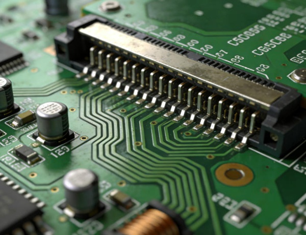
- Vias and layer transitions
- Termination and loading
Signal integrity issues arise when these elements are not carefully controlled.
When Signal Integrity Becomes a Design Concern
Signal integrity problems are primarily driven by edge rate, not clock frequency. A design should be treated as high-speed when trace length becomes electrically significant relative to the signal rise time.
Common indicators include:
- Fast rise/fall times
- Long trace lengths
- Tight timing margins
- High-density routing
Ignoring SI considerations at this stage often leads to late-stage redesigns.
Common Signal Integrity Problems in High-Speed PCBs
Reflections and Ringing
Reflections occur when impedance mismatches exist along a signal path. These mismatches are often caused by:
- Via transitions
- Trace width changes
- Connector interfaces
- Improper termination
Reflections can distort signal edges and reduce noise margins.
Crosstalk Between Adjacent Signals
Crosstalk is caused by electromagnetic coupling between nearby traces. It becomes more severe when signals run parallel over long distances or when spacing is insufficient.
Crosstalk can result in:
- Timing jitter
- False switching
- Increased noise
Proper spacing and routing discipline are essential to control crosstalk.
Return Path Discontinuities
High-speed signals always require a continuous return path. When signals cross plane splits or gaps, return currents are forced to detour, increasing loop area and noise.
Return path disruptions are a major but often overlooked source of SI and EMI problems.
🔗 Layout perspective:
High-Speed PCB Layout and Routing Best Practices
Impedance Control and Transmission Line Effects
Controlled impedance routing is fundamental to maintaining signal integrity.
Key considerations include:
- Selecting appropriate trace geometry based on stackup
- Maintaining consistent trace width and spacing
- Avoiding abrupt geometry changes
- Ensuring adjacent reference planes
Impedance should be defined early and verified with both calculation and simulation.
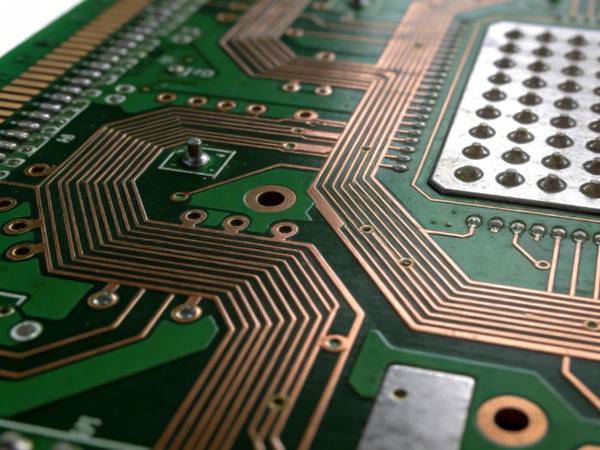
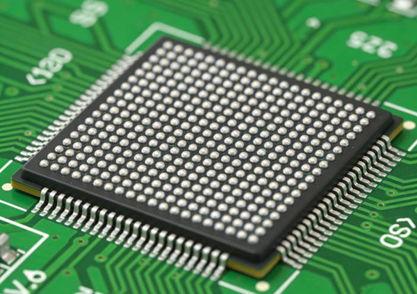
Via Effects on Signal Integrity
Vias introduce parasitic inductance and capacitance, creating impedance discontinuities.
Best practices for managing via-related SI issues include:
- Minimizing via count on critical nets
- Reducing via stubs
- Using back-drilling when required
- Aligning via strategy with stackup design
Via modeling is often necessary for very high-speed interfaces.
Termination Strategies for High-Speed Signals
Proper termination helps reduce reflections and improve signal quality.
Common termination approaches include:
- Source termination
- End termination
- Differential termination
Termination choices depend on driver strength, topology, and interface requirements.
The Role of SI Simulation and Measurement
Simulation plays a critical role in modern high-speed PCB design. SI simulation helps engineers:
- Predict reflections and crosstalk
- Evaluate impedance profiles
- Validate routing strategies before fabrication
Measurement techniques such as TDR and eye diagram analysis are used to validate real hardware.
Simulation should complement—not replace—good layout practices.
Signal Integrity and Manufacturing Considerations
Manufacturing variations can affect signal integrity. Factors such as trace width tolerance, dielectric constant variation, and layer registration all influence impedance.
Designers should:
- Communicate impedance requirements clearly
- Select materials with controlled properties
- Understand fabrication tolerances
🔗 Manufacturing perspective:
High-Speed PCB Design for Manufacturability and Yield
Best Practices Summary for SI in High-Speed PCB Design
To maintain signal integrity:
- Identify high-speed signals early
- Define and control impedance
- Maintain continuous return paths
- Minimize vias and stubs
- Validate designs through simulation and review
Signal integrity is best addressed as part of a disciplined design workflow rather than as a late-stage fix.
Conclusion
Signal integrity is a defining challenge in high-speed PCB design. By understanding transmission line behavior, controlling impedance, and maintaining proper return paths, engineers can significantly reduce signal-related issues.
This article provides a foundational reference for managing signal integrity throughout the high-speed PCB design process.
FAQ – Signal Integrity in High-Speed PCB Design
A: Signal integrity problems are caused by impedance mismatches, poor return paths, excessive vias, crosstalk, and improper termination.
A: Rise time is more important than clock frequency. Fast edges can cause SI issues even at relatively low clock rates.
A: Most high-speed digital signals benefit from controlled impedance, especially when trace lengths are significant relative to rise time.
A: Crosstalk introduces unwanted noise and timing jitter, which can degrade eye openings and cause functional failures.
A: Some issues can be mitigated, but many SI problems require layout or stackup changes, making early design discipline essential.
A: SI simulations are highly recommended for high-speed designs but are most effective when combined with good layout practices.
A: Vias introduce parasitic effects and stubs that can cause reflections, especially at very high data rates.