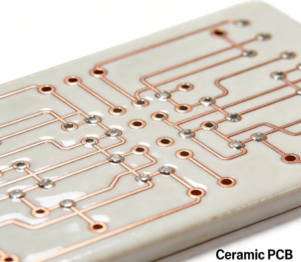
Han Sphere Blog

Explore the latest trends, technologies, and best practices in PCB design, manufacturing, and the electronics industry

High-Speed PCB Layout and Routing Best Practices

High-Speed PCB Layout and Routing Best Practices

Learn practical layout and routing best practices for high-speed PCB design, including impedance control, return paths, vias, and crosstalk management.

The Future of AI in PCB Design Automation and Electronic Manufacturing

The Future of AI in PCB Design Automation and Electronic Manufacturing

This article explores upcoming trends in AI-powered PCB design automation. It highlights deeper EDA tool integration, real-time manufacturing feedback loops, and the consequent evolution of engineering workflows, driving greater efficiency…

Innovative PCB Design Techniques for the Future

Innovative PCB Design Techniques for the Future

Discover cutting-edge trends in PCB design shaping tomorrow's electronics. This article explores flexible and multilayer boards, advanced automated testing, and key emerging technologies. Gain expert insights to master innovative techniques…

Advanced PCB Design Tips for Enhanced Efficiency and Performance

Advanced PCB Design Tips for Enhanced Efficiency and Performance

Discover advanced PCB design tips to enhance performance and reduce errors. This guide covers signal integrity techniques, effective thermal management strategies, and essential best practices for a streamlined and successful…

About Our Blog

Han Sphere Blog shares the latest trends, technologies, and best practices in PCB design, manufacturing, and the electronics industry. Our expert team regularly shares their knowledge and experience.

Popular Posts

WhatsApp