Explore essential design tips for clear and readable PCB silkscreen printing to enhance manufacturing efficiency, assembly accuracy, and troubleshooting.
When designing a Printed Circuit Board (PCB), ensuring the clarity of your silkscreen is just as crucial as routing your traces correctly. The silkscreen layer, often referred to as the legend, communicates essential information to manufacturers, automated optical inspection (AOI) machines, assemblers, and field technicians. Poorly designed silkscreens can lead to costly assembly errors, increased troubleshooting time, and overall project delays. This comprehensive guide provides actionable design tips for clear and readable PCB silkscreen printing that will elevate the quality, professionalism, and manufacturability of your boards.
Why Silkscreen Clarity Matters
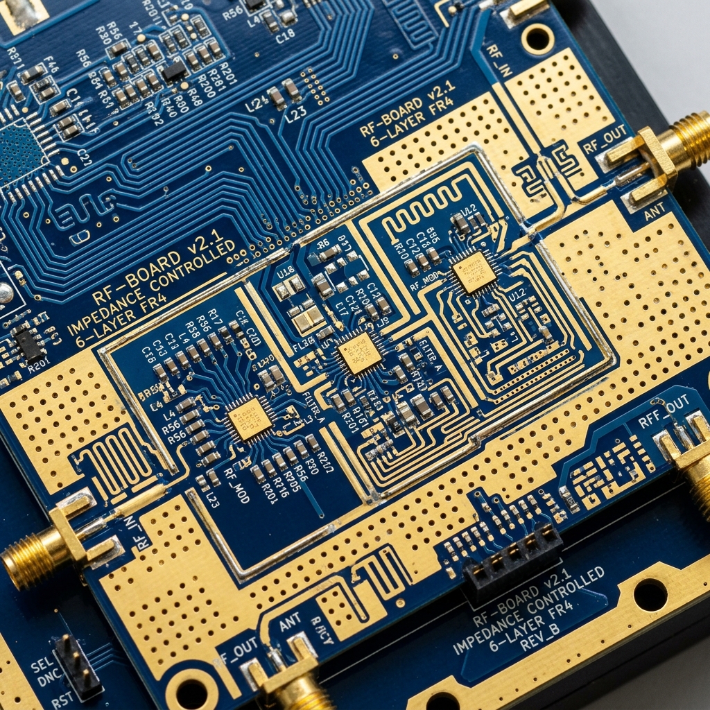
The silkscreen layer typically contains component reference designators, polarity marks, pin 1 indicators, test point labels, board identification details, and sometimes even company logos. If these elements are illegible, blurry, or missing, the risk of placing a component backward or in the wrong location skyrockets. During the debugging phase, an engineer relying on an unreadable board will waste valuable time tracing connections manually. Following established PCB manufacturing guidelines helps ensure that the silkscreen serves its primary purpose effectively, reducing both time-to-market and rework costs.
Top Design Tips for Clear Silkscreen Printing
Achieving optimal readability requires meticulous attention to font size, line width, placement strategy, and clearance rules. Here are the most critical factors and design tips for clear communication on your PCB:

1. Choose the Right Font Size and Line Width
The font size you select directly impacts the final readability of the printed legend. A common industry recommendation is to use a minimum text height of 35-40 mils (0.89-1.02 mm) and a line width (or stroke width) of at least 5 mils (0.127 mm). Fonts that are too small or thin will blur, break, or fail to print entirely during the manufacturing process, especially if the manufacturer uses lower-resolution printing methods. Conversely, fonts that are too thick may bleed together, turning an “8” into a solid blob. Choosing a simple, sans-serif vector font ensures maximum clarity and reliable Gerber generation.
2. Mind the Placement and Orientation
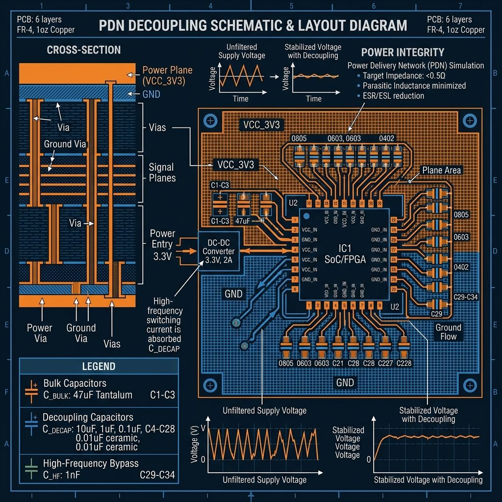
Silkscreen text should ideally be oriented in one or two directions maximum (e.g., left-to-right and bottom-to-top). This prevents the person reading the board from having to constantly rotate it in their hands to decipher the text. Place reference designators close to their corresponding components, but ensure they are not obscured when the component is actually populated. For high-density interconnect (HDI) boards, refer to advanced Các chiến lược thiết kế PCB HDI to find creative placement solutions without compromising readability. Sometimes, grouping labels and pointing to the components with silkscreen lines is necessary in extremely tight layouts.
3. Ensure Proper Clearances and Avoid Copper
One of the golden rules of PCB design is to never place silkscreen over exposed copper pads, via holes, or solder mask openings. If silkscreen ink gets onto a solder pad, it acts as an insulator and can compromise the solder joint, leading to poor electrical connections, tombstoning, or complete component failure. Most Electronic Design Automation (EDA) tools allow you to run a Design Rule Check (DRC) to automatically identify instances where silkscreen violates clearance rules. Always adhere to standard PCB assembly processes which mandate a strict separation (usually at least 2-3 mils) between ink and solderable surfaces.
4. Use Polarity and Pin 1 Indicators Effectively
For polarized components like electrolytic capacitors, diodes, LEDs, and Integrated Circuits (ICs), unambiguous markings are vital. Use standard, easily recognizable symbols (like a plus sign for tantalum capacitors, a line for diode cathodes, or a clear dot for Pin 1 on ICs) and ensure they are clearly visible after the component is soldered onto the board. A common, frustrating mistake is placing the polarity mark underneath the component body, rendering it invisible once assembly is complete.
5. Utilize Silkscreen for Test Points and Instructions
Beyond basic component identification, a well-designed silkscreen should include labels for test points, power rails (e.g., +5V, GND), and any critical handling instructions (like “ESD Sensitive”). Clear labeling of test points drastically reduces the time required for testing and quality assurance, preventing accidental shorts during probing.
How to Verify Silkscreen Clarity Before Manufacturing
Follow these systematic steps to ensure your silkscreen design will print clearly and correctly before sending your final Gerber files to the manufacturer.
-
Run Comprehensive DRC Checks
Execute your EDA tool’s Design Rule Check specifically configured for silkscreen-to-mask and silkscreen-to-copper clearances. Rigorously fix all reported errors.
-
Review Exported Gerber Files
Export your Gerber files and use an independent, third-party Gerber viewer. Inspect the silkscreen layers (typically the top overlay and bottom overlay) against the solder mask layer to visually confirm no overlaps exist.
-
Print a 1:1 Scale Paper Copy
Print the silkscreen layer at a 1:1 scale on standard paper. If you cannot read the text comfortably on the paper, it will likely be unreadable on the actual manufactured PCB.
-
Consult Your Manufacturer’s Capabilities
Check your chosen manufacturer’s specific capabilities regarding minimum text height and line width, and adjust your design rules accordingly. If you are pushing the limits of standard manufacturing, consider seeking professional DFM analysis services to validate your complex designs.
Kết luận
Implementing these design tips for clear PCB silkscreen printing is a hallmark of a professional designer. It will significantly reduce assembly errors, facilitate easier automated optical inspection, and streamline testing and debugging. By carefully managing font sizes, strictly enforcing clearances, and thoughtfully placing component indicators, you ensure that your board communicates necessary information clearly to everyone involved in its lifecycle, from the fabrication house to the end-user.
Các câu hỏi thường gặp
What happens if silkscreen is placed over a solder pad?
If silkscreen ink is inadvertently printed on a solder pad, it acts as a thermal and electrical barrier, preventing solder from adhering properly to the copper. This can lead to weak mechanical joints, tombstoning of surface-mount components, or completely failed electrical connections.
What is the minimum recommended text size for PCB silkscreen?
While printing capabilities vary by manufacturer and the printing method used (e.g., Direct Legend Printing vs. traditional screen printing), a standard safe minimum is a text height of 35-40 mils (0.89-1.02 mm) paired with a line width of at least 5 mils (0.127 mm).
Can I use custom TrueType fonts for my PCB silkscreen?
While some modern EDA tools support custom TrueType fonts, it is generally recommended to use standard, built-in vector fonts provided by the software. TrueType fonts can sometimes translate poorly into Gerber files or require complex polygon generation, potentially leading to fuzzy, bloated, or unreadable text upon fabrication.
How can I label components on a very dense board where there is no room?
On extremely dense boards, standard placement may be impossible. In these cases, you can group components and place a single silkscreen block nearby with leaders pointing to the components, or you can rely on an assembly drawing rather than trying to fit every designator on the physical board.