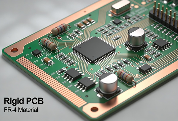
Rigid PCB layout and routing determine the electrical performance, manufacturability, and reliability of a circuit board. Even with a good stackup, poor layout choices can lead to signal integrity problems, EMI issues, and production failures.
This article explains rigid PCB layout and routing rules, focusing on practical guidelines engineers can apply in real-world designs.
🔗 Part of the Rigid PCB Design Series
Rigid PCB Design: Fundamentals, Stackup, Layout, Manufacturing, and Reliability
Key Differences Between Layout and Routing
- Layout defines component placement and functional zones
- Routing defines electrical connections and current paths
Good layout simplifies routing and improves performance.
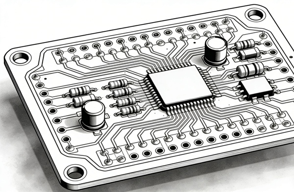
Component Placement Best Practices
Functional Zoning
Group components by function:
- Power regulation
- Signal processing
- Interfaces
Clear zoning reduces noise coupling.
Critical Component Placement
- Place connectors first
- Position power ICs near loads
- Keep sensitive components away from noise sources
Ground and Power Layout Principles
Continuous Ground Planes
- Avoid splits under high-speed signals
- Maintain uninterrupted return paths
Power Distribution Strategy
- Use planes instead of wide traces
- Minimize loop areas
- Place decoupling capacitors close to pins
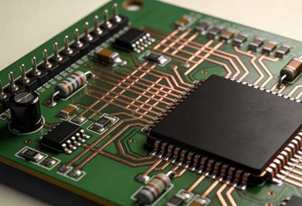
Signal Routing Rules for Rigid PCBs
Trace Width and Spacing
- Follow manufacturer design rules
- Use wider traces where possible
- Avoid pushing minimums everywhere
High-Speed Signal Routing
Best practices include:
- Route over solid reference planes
- Minimize via transitions
- Avoid stubs
Differential Pair Routing
- Maintain consistent spacing
- Match trace lengths
- Avoid unnecessary layer changes
Via Usage Guidelines
- Use through-hole vias by default
- Minimize via count
- Place stitching vias near plane transitions
Excessive vias increase impedance discontinuities.
EMI and Crosstalk Control
To reduce EMI:
- Maintain short return paths
- Use ground stitching vias
- Increase spacing between aggressive signals
Common Layout and Routing Mistakes
- Poor component placement
- Routing signals across plane splits
- Long return paths
- Excessive via usage
These mistakes often cause re-spins.
Layout and Routing Best Practices Summary
- Prioritize layout before routing
- Keep power and ground solid
- Route critical signals first
- Leave margin for manufacturing
Conclusion
Rigid PCB layout and routing rules directly affect signal integrity, EMI, and manufacturability. Applying disciplined layout principles leads to stable, reliable, and cost-effective PCB designs.
This article forms the execution core of the Rigid PCB Design content cluster.
FAQ – Rigid PCB Layout & Routing
A: Layout should always be finalized before routing.
A: Critical, especially for high-speed and sensitive signals.
A: Yes, with proper stackup and routing rules.
A: No. It increases manufacturing risk.
A: As few as possible while meeting routing needs.
A: Yes, especially in industrial and communication applications.