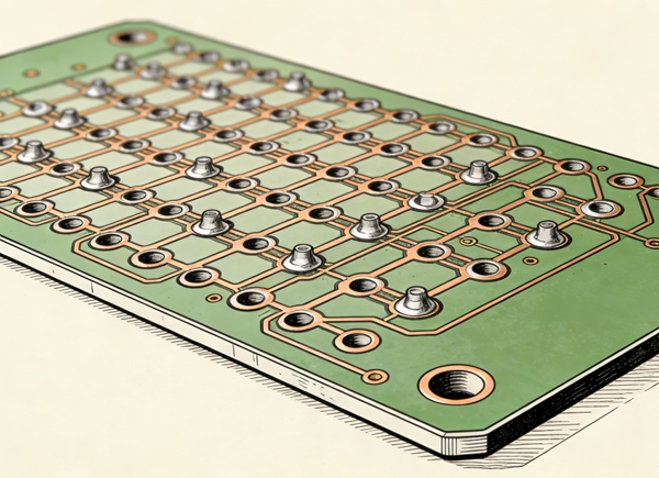
Signal integrity (SI) and power integrity (PI) are critical factors in modern rigid PCB design, especially as signal speeds and power densities continue to increase. Poor SI or PI can cause timing errors, noise, EMI, and system instability.
This article explains signal and power integrity in rigid PCB design, focusing on practical design strategies to ensure stable and reliable board performance.
🔗 Part of the Rigid PCB Design Series
Rigid PCB Design: Fundamentals, Stackup, Layout, Manufacturing, and Reliability
Why Signal Integrity Matters in Rigid PCBs
Signal integrity issues arise from:
- Impedance discontinuities
- Reflections and ringing
- Crosstalk between traces
These problems become more severe as edge rates increase.
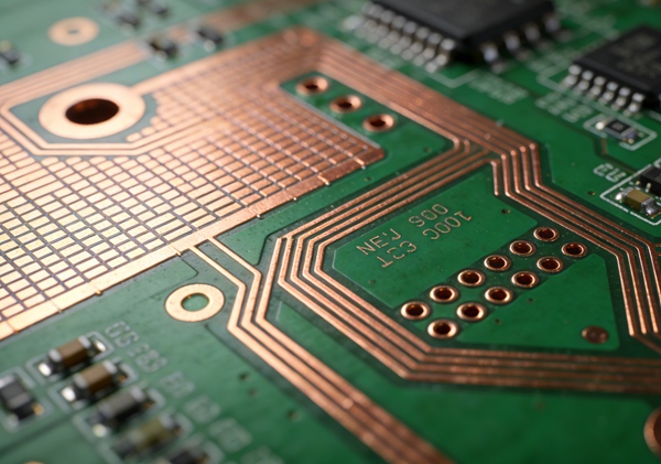
Impedance Control Basics
Key factors affecting impedance:
- Trace width
- Dielectric thickness
- Reference plane continuity
Controlled impedance must be planned at the stackup stage.
🔗 Foundation:
Rigid PCB Stackup Design and Layer Planning
High-Speed Signal Routing Considerations
Best practices include:
- Routing signals over solid reference planes
- Minimizing stubs and via transitions
- Avoiding sharp corners
Shorter, cleaner paths improve signal quality.
Crosstalk and Noise Reduction
To minimize crosstalk:
- Increase spacing between parallel traces
- Route adjacent layers orthogonally
- Use ground shielding where necessary
Power Integrity Fundamentals
Power integrity ensures stable voltage delivery under dynamic load conditions.
Common PI issues include:
- Voltage droop
- Ground bounce
- Switching noise
Power Distribution Network (PDN) Design
Effective PDN design involves:
- Solid power and ground planes
- Proper decoupling capacitor placement
- Low-inductance current paths
Plane-based PDNs outperform trace-based approaches.
Decoupling and Bypass Capacitors
Best practices:
- Place decoupling caps close to IC power pins
- Use multiple capacitor values
- Minimize loop area
Decoupling effectiveness depends heavily on layout.
Return Path and Reference Planes
Signal return currents:
- Follow the path of least impedance
- Require continuous reference planes
Broken return paths increase EMI and noise.
Common SI/PI Design Mistakes
- Ignoring return path continuity
- Overusing vias on critical signals
- Poor decoupling strategy
These often cause late-stage failures.
Best Practices Summary
- Define impedance early
- Use solid planes for power and ground
- Route critical signals first
- Validate designs with simulation when needed
Conclusion
Signal and power integrity are essential for reliable rigid PCB performance. By addressing SI and PI at the design stage, engineers can prevent many common issues and ensure robust system operation.
This article establishes the performance authority layer of the Rigid PCB Design content cluster.
FAQ – Signal & Power Integrity in Rigid PCB Design
A: Yes, especially for high-speed signals.
A: Yes. PI and SI are closely related.
A: Strongly recommended for modern designs.
A: Depends on IC requirements and power demand.
A: Not always, but useful for high-speed or sensitive designs.
A: Yes, with proper stackup and routing.