Testing problems often start in layout.
A PCB reaches production and suddenly:
- ICT cannot access key signals
- flying probe coverage is limited
- debugging takes too long
The board may be manufacturable.
But: it is not testable.
That’s where DFT (Design for Testability) becomes important.
Good DFT makes testing:
- nhanh hơn
- cheaper
- more reliable
And more importantly:
it prevents expensive surprises during production.
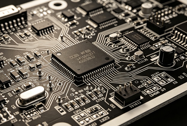
What Is Design for Testability (DFT)?
DFT means designing the PCB so it can be tested effectively during manufacturing and debugging.
Instead of adding testing later, DFT is considered during:
- schematic design
- PCB layout
- assembly planning
The goal:
maximize fault detection while minimizing testing difficulty.
Why DFT Matters
Poor testability causes problems like:
- low test coverage
- difficult debugging
- higher production cost
- slower troubleshooting
In production:
fixing testability problems after layout is expensive.
Good DFT improves:
- hiệu quả sản xuất
- defect detection
- product reliability
Overview: Giải thích về các phương pháp kiểm tra PCB
Common PCB Testing Challenges
Many problems repeat across projects.
Các vấn đề thường gặp bao gồm:
- inaccessible test points
- crowded layouts
- hidden signals
- poor connector access
- missing debug interfaces
These issues are usually design-related.
Key DFT Rules for PCB Design
1. Add Enough Test Points
This is the most important rule.
Without test points:
- ICT becomes difficult
- flying probe slows down
- debugging becomes frustrating
Thực tiễn tốt nhất:
Add test points for:
- power rails
- ground
- critical signals
- communication buses
Test Point Placement Tips
Avoid placing test points:
- under components
- near tall parts
- in inaccessible areas
Maintain enough spacing for probes.
2. Plan for ICT Access
ICT requires physical contact.
That means:
probe access must exist.
Hãy xem xét:
- probe spacing
- fixture clearance
- component height restrictions
Xem thêm: Kiểm tra bằng công nghệ ICT so với kiểm tra bằng đầu dò bay: Phương pháp kiểm tra PCB nào tốt hơn?
3. Include Debug Interfaces
Debugging becomes much easier with access.
Common interfaces:
- UART
- JTAG
- SWD
- programming headers
Even temporary debugging pads help.
4. Label Critical Signals Clearly
Good silkscreen saves engineering time.
Helpful labels:
- power rails
- reset pins
- debug interfaces
This sounds simple—but helps during troubleshooting.
5. Separate Dense Components
Overcrowded placement causes testing issues.
Leave reasonable access around:
- đầu nối
- ICs
- critical test locations
6. Design for Functional Testing
Think beyond electrical testing.
Ask:
“How will this board actually be tested?”
Hãy xem xét:
- fixture interface
- communication ports
- LEDs or indicators
- diagnostic firmware
Xem thêm: Kiểm thử chức năng trong quá trình lắp ráp bảng mạch in (PCB)
7. Add Ground Reference Points
Measurements become easier with:
- accessible ground pads
- stable probing reference
Especially important during debugging.
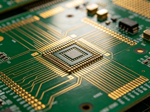
DFT for Different Testing Methods
DFT for ICT
Focus on:
- accessible test pads
- probe spacing
- fixture compatibility
DFT for Flying Probe
Focus on:
- reachable nets
- sufficient probe access
Flying probe is more flexible than ICT.
DFT for Functional Testing
Focus on:
- software hooks
- debug ports
- communication interfaces
DFT vs DFM vs DFA
These terms are often confused.
| Term | Meaning | Focus |
|---|---|---|
| DFT | Design for Testability | easier testing |
| DFM | Design for Manufacturability | easier fabrication |
| DFA | Design for Assembly | easier assembly |
Good PCB design usually considers all three.
Cách cải thiện khả năng kiểm tra của bảng mạch in (PCB)
- 1. Review Test Strategy Early
Testing should be planned before layout.
- 2. Involve Manufacturing Teams
PCB assemblers often spot DFT risks early.
- 3. Build Prototype Testing First
Use prototypes to validate:
. coverage
. access
. fixture concept - 4. Standardize Test Access
Consistent placement helps production efficiency.
Common DFT Mistakes
Các vấn đề thường gặp trong quá trình sản xuất:
- forgetting test points
- inaccessible debug signals
- no fixture clearance
- dense placement blocking probes
- relying only on AOI inspection
Testing problems often become expensive redesigns.
Những lưu ý thực tiễn từ quá trình sản xuất thực tế
What commonly happens:
- prototype boards expose missing test access quickly
- ICT failures are often layout-related
- debug connectors save huge amounts of engineering time
- DFT planning reduces production troubleshooting dramatically
The cheapest time to think about testing is during layout.
Kết luận
Design for Testability (DFT) helps ensure a PCB can be tested efficiently throughout manufacturing and debugging.
By planning test points, probe access, and debug interfaces early, engineers can improve fault coverage, reduce troubleshooting time, and lower production cost.
Good testing starts long before production—it starts in design.
FAQ
A: DFT stands for Design for Testability, which means designing a PCB for easier testing.A:
A: They allow ICT, flying probe, and debugging access.
A: DFT focuses on testing, while DFM focuses on manufacturability.
A: Yes, but the level of DFT depends on product complexity and production volume.
A: As early as schematic and layout design stages.