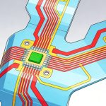
Rigid PCB manufacturing success depends not only on electrical design but also on how well the design aligns with fabrication and assembly processes. Design for Manufacturability (DFM) ensures high yield, stable quality, and predictable cost.
This article explains rigid PCB manufacturing, DFM, and assembly considerations, helping engineers avoid common production pitfalls.
🔗 Part of the Rigid PCB Design Series
Rigid PCB Design: Fundamentals, Stackup, Layout, Manufacturing, and Reliability
Overview of the Rigid PCB Manufacturing Process
Key fabrication steps include:
- Material preparation
- Imaging and etching
- Drilling and plating
- Lamination
- Solder mask and surface finish
Each step introduces constraints that designers must respect.
Core DFM Principles for Rigid PCBs
Standard Design Rules
- Follow fabricator minimum trace/space
- Use standard via sizes
- Avoid unnecessary complexity
Standard rules improve yield and reduce cost.
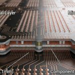
Stackup and Copper Balance
- Maintain symmetric stackups
- Balance copper distribution
This prevents warpage during lamination and assembly.
Via Design and Drilling Considerations
Best practices:
- Use through-hole vias where possible
- Avoid excessive via aspect ratios
- Keep via sizes within fab capability
Poor via design leads to plating failures.
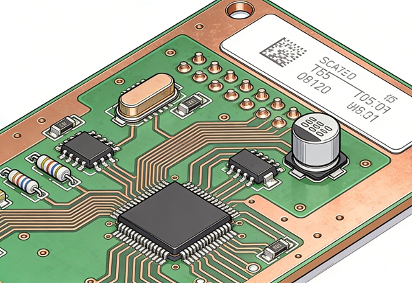
Solder Mask and Assembly Constraints
Solder Mask Openings
- Avoid overly tight mask dams
- Ensure mask alignment tolerance
Component Spacing
- Allow sufficient spacing for assembly
- Consider rework access
Crowded layouts increase assembly defects.
Surface Finish Selection
Common finishes include:
- HASL
- ENIG
- OSP
Each affects solderability, cost, and reliability.
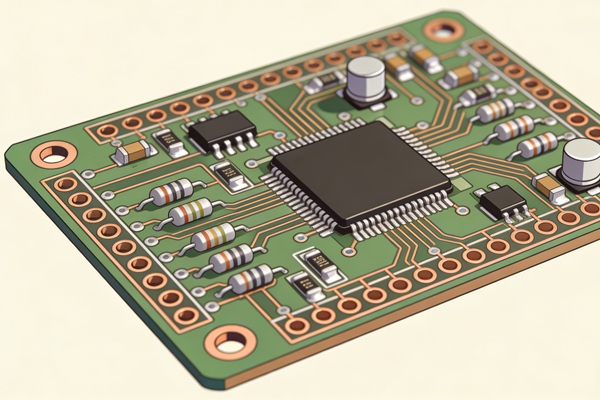
Panelization and Board Outline
Manufacturing-friendly design includes:
- Smooth board outlines
- Adequate panel rails
- Fiducials for alignment
Poor panelization increases handling damage.
Common Manufacturing and Assembly Issues
Typical issues include:
- Solder bridging
- Warpage during reflow
- Misregistration
Most are preventable through DFM.
Best Practices Summary
- Engage manufacturers early
- Design with standard rules
- Validate stackup and via structures
- Consider assembly from day one
Conclusion
Rigid PCB manufacturing success depends on thoughtful DFM and assembly-aware design. By aligning design decisions with fabrication capabilities, engineers can achieve reliable, scalable production.
This article establishes the production-readiness layer of the Rigid PCB Design cluster.
FAQ – Rigid PCB Manufacturing & DFM
A: Design practices that improve manufacturability and yield.
A: From the earliest design stages.
A: They increase cost and risk unless truly necessary.
A: ENIG is widely used for its reliability.
A: Yes, especially with unbalanced stackups.
A: Absolutely. Fabrication and assembly are tightly linked.