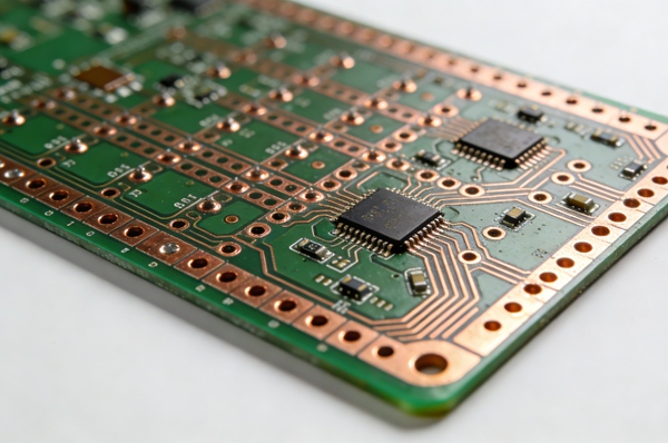
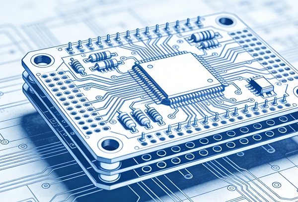
Signal and Power Integrity in Rigid PCB Design
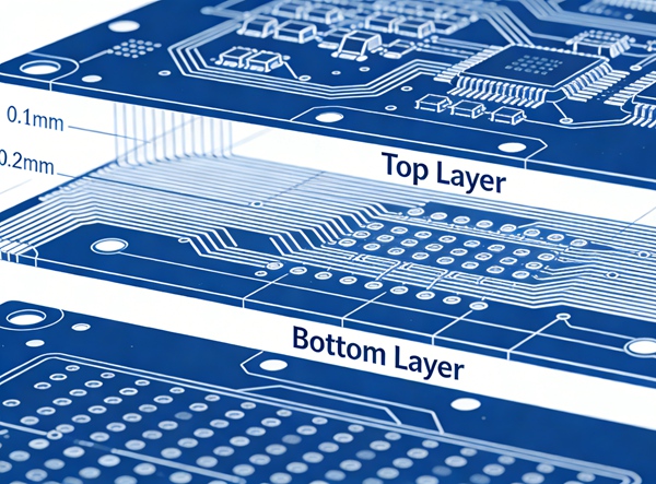
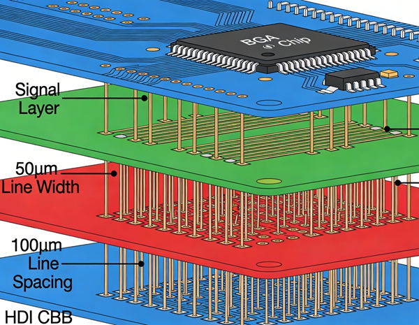
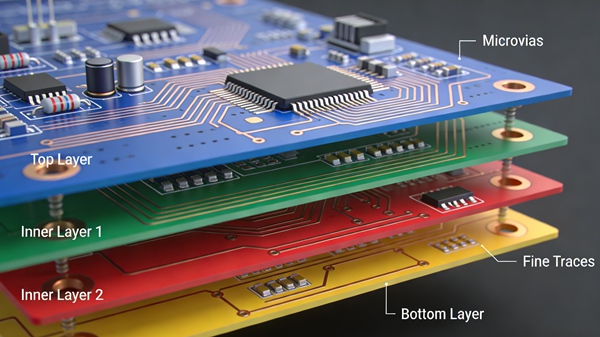
This article explores key signal and power integrity principles for rigid PCB design. It covers essential topics including controlled impedance for signal traces, robust power distribution network (PDN) design, effective…