If high-speed design starts anywhere, it starts with the stackup.
Not routing. Not placement.
Stackup.
Once the layer structure is fixed, most of your electrical behavior is already constrained:
- trở kháng
- đường truyền ngược
- nhiễu chéo
- loss
Trying to “fix” these later in layout is usually painful.
What Stackup Really Controls
A PCB stackup defines:
- where signals are routed
- where reference planes are placed
- how fields are contained
In practice, it determines:
- độ ổn định trở kháng
- EMI performance
- routing flexibility
If the stackup is weak, everything downstream becomes harder.
Basics: Hướng dẫn thiết kế cấu trúc lớp PCB FR4
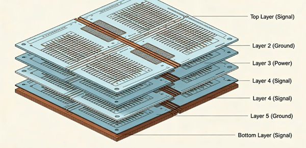
Typical 6-Layer Stackup
A common 6-layer structure:
L1  Signal
L2  Ground
L3  Signal
L4  Signal / Power
L5  Ground
L6  Signal
Where it works
- moderate-speed designs
- cost-sensitive products
- limited routing density
Hạn chế
- fewer reference planes
- more signal layers competing for routing
- harder to isolate noisy signals
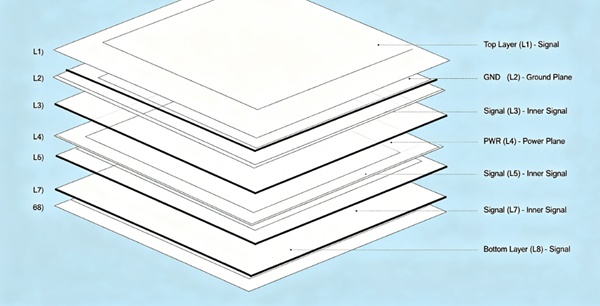
Typical 8-Layer Stackup
A common 8-layer structure:
L1  Signal
L2  Ground
L3  Signal
L4  Power
L5  Ground
L6  Signal
L7  Ground
L8  Signal
Ưu điểm
- better signal/plane pairing
- improved return path control
- reduced crosstalk
Practical impact
Most high-speed designs start to feel “comfortable” at 8 layers.
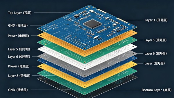
Typical 10-Layer Stackup
A common 10-layer structure:
L1  Signal
L2  Ground
L3  Signal
L4  Ground
L5  Signal
L6  Signal
L7  Ground
L8  Signal
L9  Ground
L10 Signal
Ưu điểm
- excellent signal isolation
- more routing channels
- strong EMI performance
Trade-offs
- chi phí cao hơn
- more complex fabrication
6 vs 8 vs 10 Layers (Quick Comparison)
| Tính năng | 6-Layer | 8-Layer | 10-Layer |
|---|---|---|---|
| kiểm soát trở kháng | basic | stable | rất ổn định |
| crosstalk control | hạn chế | tốt | xuất sắc |
| mật độ định tuyến | vừa phải | cao | rất cao |
| EMI performance | vừa phải | tốt | in đậm |
| chi phí | thấp hơn | trung bình | cao hơn |
How Layer Count Affects Signal Integrity
1. Return Path Quality
More planes → better return paths
Xem: Đường dẫn hồi và mặt phẳng nối đất trên bảng mạch in (PCB) trong thiết kế tốc độ cao
2. Crosstalk
More spacing + better shielding → less coupling
3. Impedance Stability
More controlled dielectric spacing → more consistent impedance
Xem: Controlled Impedance PCB Design: How to Achieve 50Ω and 100Ω
4. Insertion Loss
Indirect effect:
- better routing → shorter paths
- cleaner structure → fewer discontinuities
Xem: Giải thích về tổn hao chèn trong PCB (Tổn hao điện môi so với tổn hao dẫn điện)
How to Choose Between 6, 8, and 10 Layers
This is usually not just a technical decision—it’s a trade-off.
- 1. Look at Signal Speed First
low–mid speed → 6 layers may work
high-speed / multi-Gbps → 8 or more - 2. Evaluate Routing Density
If routing is congested:
adding layers is often easier than forcing layout - 3. Check Power Distribution Needs
More planes → better power integrity
- 4. Consider EMI Requirements
Stricter EMI → more layers + better shielding
- 5. Balance Cost vs Risk
Fewer layers save cost—but increase design risk.
More layers increase cost—but simplify SI/EMI control.
How to Build a Good High-Speed Stackup
This is where designs succeed.
1. Pair Signal Layers with Planes
Every signal layer should have a nearby reference plane.
2. Use Symmetrical Structures
Balanced stackups reduce warping and improve manufacturability.
3. Keep Dielectric Thickness Consistent
Helps maintain stable impedance.
4. Separate High-Speed and Noisy Signals
Use different layers or shielding planes.
5. Plan Via Transitions Early
Layer changes introduce discontinuities.
Details: Thiết kế lỗ thông qua (Via) trên bảng mạch in (PCB) trong các mạch tốc độ cao
Microstrip vs Stripline in Stackup
- outer layers → microstrip
- inner layers → stripline
Stripline advantages:
- less EMI
- khả năng che chắn tốt hơn
- trở kháng ổn định hơn
High-speed signals are often routed on inner layers for this reason.
Những lưu ý thiết kế thực tiễn
What usually happens in real projects:
- 6-layer designs often become 8-layer after SI review
- 8-layer is the “sweet spot” for many products
- 10-layer is common for high-density or high-speed systems
- stackup decisions made early save redesign time later
Kết luận
Stackup design defines the electrical behavior of a high-speed PCB.
While 6-layer boards can work for simpler designs, 8-layer and 10-layer structures provide better control over impedance, return paths, and crosstalk.
Choosing the right layer count is a balance between performance, routing complexity, and cost—but getting the stackup right early makes everything else easier.
FAQ
A: It can be, but it becomes harder to control impedance and crosstalk compared to 8-layer designs.
A: It provides a good balance between performance, routing flexibility, and cost.
A: For high-speed, high-density, or EMI-sensitive designs.
A: Not always, but more layers usually make it easier to control signal integrity.
A: Yes. Stackup should be defined before layout begins.