High-Frequency PCB
(RF / Microwave)
Rogers, Taconic and PTFE laminates from 1 GHz to 110 GHz — stocked in-house, processed in-house, and TDR + VNA verified before every shipment.
The board technology that makes RF systems actually work
A high-frequency PCB is built on purpose-designed low-loss laminate — Rogers, Taconic, PTFE or ceramic-filled PTFE — instead of standard FR4. The laminate choice is not a preference. At frequencies above 1 GHz, standard FR4 introduces signal loss and impedance variance that degrades system performance in ways that cannot be compensated by circuit design.
At 10 GHz, a trace on Rogers 4350B has approximately 5× less loss than the same trace on FR4. At 77 GHz — used for automotive radar — FR4 is not a usable transmission medium. The physics of high-frequency signal propagation make laminate selection a critical design decision, not a procurement variable.
Our RF engineers specify the right laminate for your frequency band, thermal environment and cost target — then fabricate, verify with TDR and optionally with VNA before shipment.
Get RF PCB Quote →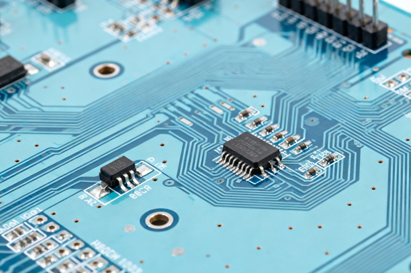
Why FR4 fails at high frequencies — and what the data shows
The physics of dielectric loss and Dk variance make laminate selection the most important RF PCB design decision.
Dielectric Loss — FR4 vs Rogers 4350B at 10 GHz
FR4's loss tangent (tan δ) of 0.020–0.025 causes signal attenuation of 1–3 dB/cm at 10 GHz. Rogers 4350B has tan δ = 0.0037 — approximately 6× lower loss at the same frequency and geometry. For a 5G base station power amplifier, this difference directly translates to efficiency, thermal dissipation and operating cost at scale.
tan δ FR4 = 0.022 · Rogers 4350B = 0.0037 · 6× less attenuationDk Variance — Why FR4 Impedance Is Unpredictable
FR4's dielectric constant varies from 4.2 to 4.8 between suppliers and even between production lots from the same supplier. A 50 Ω trace designed to nominal Dk = 4.4 can be 44 Ω or 57 Ω on a different FR4 lot — before fabrication tolerance is even considered. Rogers 4350B has Dk = 3.48 ±0.05 — tight enough to design to with confidence.
FR4 Dk variance ±0.3 · Rogers 4350B Dk = 3.48 ±0.05Hybrid Stackup — RF Performance at Controlled Cost
Most RF + digital mixed designs do not need Rogers on every layer. Outer layers handling RF traces use Rogers or PTFE for signal performance. Inner digital layers handling clocks, power and data buses use standard FR4 at standard cost. Our hybrid stackup design service specifies which layers need low-loss laminate and which do not — optimising performance per dollar.
Rogers outer layers · FR4 inner layers · hybrid stackup · cost optimisedFull high-frequency PCB specification
All RF laminates stocked in-house. TDR impedance report supplied with every controlled-impedance order. VNA S-parameters available on request.
Parameter für die Herstellung
| Max Operating Frequency | Up to 110 GHz (Rogers 3003C / PTFE) |
| Impedanztoleranz | ±5% TDR verified (±3% on precision orders) |
| RF Laminates | Rogers 4350B · RO4003C · RO3003C · Taconic TLY · PTFE |
| Anzahl der Schichten | 2 - 30 Schichten |
| Min. Spur/Leerzeichen | 2.5 / 2.5 mil (RF: ±0.5 mil tolerance) |
Leistung und Standards
| Oberfläche | ENIG · ENEPIG · Electrolytic Hard Gold |
| Cavity Milling | Waveguide integration · connector pockets |
| Back-Drill | Via stub removal for high-speed digital layers |
| Überprüfung | TDR standard · VNA S-parameters on request |
| Prototype Turnaround | 48h express · 5 days standard |
How high-frequency PCB is fabricated
RF PCB fabrication combines tighter process tolerances and RF-specific verification steps not present in standard PCB manufacturing.
Laminate Selection & Inspection
Rogers, Taconic or PTFE laminate is selected per Dk, tan δ and CTE requirements. Incoming Dk is verified against CoC before production begins.
Tight-Tolerance Imaging & Etch
Trace width is held to ±0.5 mil (vs ±1 mil on FR4) using optimised photolithography parameters. Verified by SEM measurement on every lot.
Cavity Milling & Drilling
Precision CNC milling creates waveguide transitions and connector pockets for mmWave boards. Laser drilling for microvias in hybrid stackups.
TDR / VNA Verification
Every board is TDR-measured for impedance. VNA S-parameter characterisation (insertion loss vs frequency) is available on all boards.
Where high-frequency PCB is the required technology
Applications where standard FR4 introduces unacceptable signal loss or impedance variance.
5G Base Station RF
Rogers/PTFE boards for 5G NR sub-6 GHz and mmWave radio units — power amplifiers and antenna feeds.
Automotive Radar
77 GHz ADAS radar front-ends on Rogers 4350B — forward collision, lane departure and blind-spot systems.
Microwave Backhaul
6–86 GHz point-to-point backhaul radios used in mobile network infrastructure.
Electronic Warfare
Wideband RF boards for ESM, jamming and signal intelligence systems across multi-octave frequency ranges.
Satellite Communications
Ka/Ku-band transceiver boards for LEO/GEO satellite payload electronics and VSAT terminals.
Spectrum Analysers & VNAs
Low-phase-noise RF front-ends for test instruments operating DC to 110 GHz.
Medizinische Bildgebung
GHz-range RF boards for MRI gradient coil drivers and medical radar (breathing/vital signs detection).
Industrial Radar Sensors
60 GHz and 77 GHz boards for industrial presence sensing, level measurement and gesture detection.
RF quality verified with RF instruments — not just optical.
Optical inspection confirms copper is present. TDR confirms impedance is correct. VNA confirms insertion loss meets your link budget. For high-frequency boards, we apply all three — because every unverified PCB variable becomes a variable in your RF system.
- ISO 9001 : 2015Von Dritten geprüftes Qualitätsmanagement
- Material CoCRogers / Taconic / PTFE Dk and tan δ per lot
- IPC-A-600 Class 2 / 3RF PCB acceptability criteria
- RoHS / REACHEinhaltung der EU-Vorschriften für gefährliche Stoffe
Inspektions- und Prüfverfahren
- TDR Impedance — All Controlled Structures±5% verified per board, report included
- VNA S-Parameter CharacterisationInsertion loss vs frequency — on request
- 100% Elektrischer Test - Fliegender TastkopfAll nets verified
- 100% AOI - Alle LagenAutomatisierte optische Inspektion
- Trace Width Measurement — SEMStatistical SPC data per lot
- Dk Verification — Material CouponPer lot, Rogers / Taconic spec check
- ENIG-Dicke - XRFNi/Au uniformity on RF contact areas
- Cavity Depth VerificationMilled pocket depth ±0.05 mm
High-frequency boards we have built
Real RF PCB challenges — material expertise and process precision delivered.
77 GHz ADAS Radar Front-End
8-layer Rogers 4350B, 128 antenna feed lines TDR-verified ±4.2%, ENIG, -40°C to +85°C, IATF 16949 documentation.
All antenna feeds within specification. RF system test exceeded simulation by +0.8 dB antenna gain. IATF 16949 FAI accepted at first submission.
28 GHz 5G Beamforming Board
12-layer hybrid Rogers 4350B / FR4, 64T64R massive MIMO, cavity-milled patch antenna apertures, 0.5 mm BGA beamforming IC fan-out.
RF system test exceeded simulation. On-time delivery for 3 consecutive production quarters. Customer qualified HanSphere as preferred supplier for 39 GHz programme.
67 GHz VNA RF Front-End Board
20-layer Rogers 3003C, cavity-milled waveguide transitions, electrolytic hard gold on RF interfaces, VNA-characterised per board.
Insertion loss within 0.3 dB of simulation at 67 GHz. All boards shipped with individual VNA data files. 100% pass at instrument calibration without RF rework.
Common questions about High-Frequency PCB
Technical questions about RF laminate selection, impedance control and fabrication.
We hold in-house stock of: Rogers 4350B (Dk 3.48, tan δ 0.0037), RO4003C (Dk 3.55, tan δ 0.0027), RO3003C (Dk 3.00, tan δ 0.0013), Taconic TLY (Dk 2.17, tan δ 0.0009), Taconic RF-35 (Dk 3.50, tan δ 0.0018), and PTFE-based laminates for frequencies above 40 GHz. Material CoC with Dk and tan δ per lot is supplied with every order.
Our standard RF impedance tolerance is ±5%, verified by TDR measurement and reported per board. For precision applications (test instruments, VNA boards, precision phase-matched lines), ±3% tolerance is available — this requires ±0.5 mil trace width control and Dk-verified laminate selection. Specify your required tolerance at enquiry stage.
Yes — full 2-port VNA S-parameter measurements (S11, S21 insertion loss vs frequency) are available on all boards as an optional service. The measurement data is supplied as Touchstone (.s2p) files and can be imported directly into your RF simulation software for correlation to design intent. Specify VNA measurement at enquiry stage.
Our standard Rogers 4350B and RO4003C process supports applications to approximately 40 GHz. For W-band (75–110 GHz) applications, we use Rogers RO3003C or PTFE-based laminates with cavity milling for waveguide integration. The practical upper limit depends on laminate choice, copper surface roughness at mmWave frequencies, and connector interface geometry.
A hybrid stackup uses low-loss RF laminate (Rogers, PTFE) on the outer layers where RF traces are routed, and standard FR4 or high-Tg laminate on inner layers for digital power and data signals. This provides RF performance where the signal quality matters (outer RF traces) while significantly reducing cost vs all-Rogers construction. Our RF engineers design hybrid stackups routinely for 5G and ADAS radar applications.
Yes — CNC cavity milling is a standard service for mmWave boards requiring recessed connector launch areas, waveguide transitions and heat spreader pockets. Cavity depth tolerance is ±0.05 mm, wall verticality ±2°. Cavity drawings should be provided as a separate mechanical layer in the Gerber/ODB++ package. Photographs and dimensional inspection reports are available on cavity lots.
Get your RF PCB design reviewed — today.
Send your Gerbers and stackup requirements. Our RF engineers review laminate selection, trace geometry and via placement within 8 hours.
- DFM-Prüfung bei jeder Anfrage inbegriffen
- NDA auf Anfrage unterzeichnet - gängige Praxis
- Antwort innerhalb von 8 Arbeitsstunden
- 48-Stunden-Express-Prototyp verfügbar
- Unverbindliches Angebot anfordern
Angebot anfordern
Füllen Sie die nachstehenden Felder aus, und wir werden uns in Kürze mit Ihnen in Verbindung setzen.