Designing a high-speed PCB is rarely about solving one problem.
A board may pass design rule checks but still experience signal reflections, unstable power rails, excessive EMI, or poor manufacturing yield. In most cases, these issues can be traced back to decisions made early in the design process.
Using a structured checklist before releasing Gerber files helps reduce design revisions and improves first-pass success.
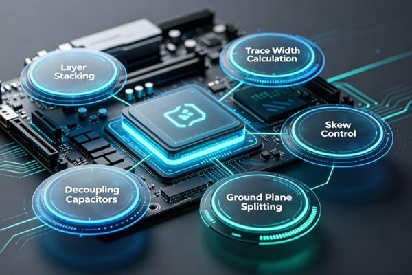
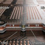
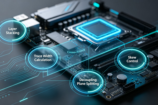
Start with the PCB Stackup
The stackup should be finalized before routing begins.
The layer arrangement determines:
- signal reference planes
- impedance stability
- routing efficiency
- power distribution
Changing the stackup after routing usually leads to unnecessary redesign work.
For more guidance, see High-Speed PCB Stackup Design (6-Layer vs 8-Layer vs 10-Layer).
Define Controlled Impedance Requirements
If the design includes high-speed interfaces, impedance requirements should be confirmed before layout.
Typical examples include:
- 50Ω single-ended traces
- 100Ω differential pairs
Work with your PCB manufacturer to verify the stackup and trace geometry instead of relying only on calculator results.
Related reading: Controlled Impedance PCB Design.
Verify Reference Planes
Every critical signal should have a continuous reference plane.
Avoid routing signals across:
- plane splits
- large voids
- discontinuous ground areas
A continuous return path reduces impedance discontinuities and minimizes unwanted radiation.
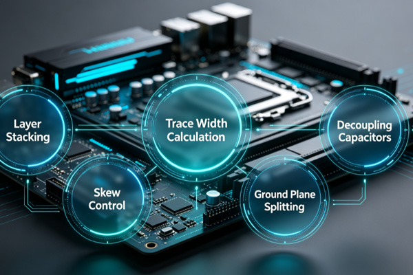
Review Differential Pair Routing
Differential pairs should remain consistent throughout the layout.
Check for:
- matched trace lengths
- constant spacing
- minimal skew
- consistent reference planes
Frequent changes in spacing or unnecessary vias can degrade signal quality.
Reduce Via Transitions
Every via changes the electrical path.
Although vias are unavoidable, excessive layer changes increase:
- impedance discontinuities
- insertion loss
- signal reflections
Critical signals should remain on the same layer whenever practical.
Related reading: PCB Via Design in High-Speed Circuits.
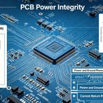
Evaluate Power Distribution
Power integrity should be reviewed alongside signal integrity.
Confirm that:
- decoupling capacitors are placed close to IC power pins
- power and ground planes are continuous
- return current paths remain short
Stable power delivery improves overall system performance.
Related reading: PCB Power Integrity Design.
Check Routing Density
Dense routing often creates manufacturing and testing problems.
Review:
- trace spacing
- copper balancing
- component clearance
- fan-out strategy
Adding another signal layer is often a better solution than forcing traces through crowded areas.
Consider Manufacturing Requirements
Before releasing manufacturing data, verify that the design is practical to fabricate.
Review items such as:
- minimum trace width
- minimum spacing
- via sizes
- annular rings
- solder mask clearance
Early DFM checks reduce production risk and improve yield.
Related reading: High-Speed PCB Design for Manufacturing & Yield.
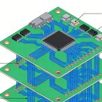
Prepare the PCB for Testing
Testing should not be treated as the final step.
Confirm that the design includes:
- accessible test points
- programming interfaces
- debugging connections
- sufficient probe clearance
These features simplify inspection and troubleshooting during production.
Perform a Final Design Review
Before generating production files, complete a comprehensive review.
Questions worth asking include:
- Are all impedance-controlled traces identified?
- Do critical signals have uninterrupted reference planes?
- Are differential pairs routed consistently?
- Is the power distribution network complete?
- Are manufacturing capabilities confirmed?
- Has the PCB been reviewed for testing accessibility?
A structured review often identifies issues that automated design rule checks cannot.
Follow a Practical Verification Process
- Step 1
Finalize the PCB stackup and confirm material selection.
- Step 2
Verify impedance requirements with the PCB manufacturer.
- Step 3
Review signal routing, return paths, and via transitions.
- Step 4
Check power distribution, decoupling placement, and reference planes.
- Step 5
Perform DFM and DFT reviews before releasing manufacturing files.
Common Design Oversights
Some of the most common issues found during PCB reviews include:
- defining the stackup after routing has started
- routing high-speed signals across split planes
- adding unnecessary vias to critical nets
- placing decoupling capacitors too far from IC pins
- releasing production data without a complete design review
Most of these issues can be avoided with a consistent review process.
Conclusion
High-speed PCB performance depends on decisions made throughout the design process, not just during routing.
By reviewing stackup, impedance, return paths, power integrity, manufacturability, and testing before production, engineers can reduce design iterations and improve product reliability.
A well-organized checklist helps identify potential issues early, when they are still easy and inexpensive to correct.
FAQ
A: Stackup planning is one of the most important steps because it affects impedance, return paths, and routing strategy.
A: Trace width and spacing depend on the selected stackup. Changing these parameters later often requires layout revisions.
A: There is no fixed number, but unnecessary vias should be avoided because each transition introduces additional discontinuities.
A: Design rule checks verify predefined rules, but they cannot evaluate every signal integrity, manufacturability, or testing consideration.
A: Both reviews should be completed before generating manufacturing files to reduce production issues and improve testing efficiency.