Choosing the right PCB surface finish is one of the most consequential decisions in printed circuit board manufacturing. The surface finish protects the exposed copper pads from oxidation, ensures reliable solderability, and directly influences the performance and longevity of your assembled board. Yet many engineers and procurement teams treat it as an afterthought—defaulting to whatever the factory recommends rather than selecting the finish that best suits their application’s requirements.
In this guide we break down the three most widely specified PCB surface finishes—HASL(熱風はんだレベリング), ENIG(無電解ニッケル・浸漬金)、および OSP(有機はんだ付け性保持剤)—covering their processes, advantages, limitations, cost implications, and the application scenarios where each one excels. Whether you are sourcing boards from a PCBの直営工場 あるいは、~に取り組む PCBサプライヤー、表面仕上げについて理解を深めることで、より適切な仕様書を作成し、より高品質な基板を入手できるようになります。
PCBの表面処理とは何か、そしてなぜ重要なのか?
Bare copper oxidizes rapidly when exposed to air, forming a layer of copper oxide that severely degrades solderability. A surface finish is a metallic or organic coating applied over the exposed copper features—pads, vias, and test points—to prevent this oxidation and maintain the copper in a solderable state from fabrication through assembly.
酸化防止以外にも、表面仕上げは以下の点に影響を与えます:
- はんだ接合部の品質 — wetting angle, void formation, and intermetallic compound thickness
- 保存期間 — how long boards remain solderable after fabrication
- 平面度 — critical for fine-pitch BGA and QFN components
- RoHS準拠 — lead-free requirements dictate which finishes are permissible
- 総費用 — finish cost is a significant line item, especially for high-volume orders
あなたがそのたびに PCBメーカーを選ぶ、表面仕上げは、彼らがまず最初に求める仕様の一つです。上流工程で正しく仕上げておけば、下流工程でのコストのかかる手直しを防ぐことができます。
HASL:熱風はんだレベリング
HASLプロセス
HASLでは、素基板を溶融はんだ槽に浸漬した後、熱風ナイフを通過させて余分なはんだを吹き飛ばし、露出したすべての銅表面に薄く均一なはんだ被膜を残します。従来のHASLではスズ・鉛(Sn63/Pb37)合金が使用されますが、鉛フリーHASL(LF-HASL)では、RoHS要件を満たすために、通常SAC305(Sn96.5/Ag3/Cu0.5)またはSnCu合金が使用されます。
HASLのメリット
- 優れたはんだ付け性 — the finish is itself solder, so it wets readily during reflow
- 長期保存が可能 — typically 12 months or more before solderability degrades
- 低コスト — the process is mature and high-throughput
- 再加工可能 — boards can be reflowed multiple times without finish degradation
- 長期保存に耐える — commonly specified for industrial and MRO applications
HASLの限界
- 平面度の低さ — the hot-air leveling process leaves slightly uneven surfaces; this is problematic for fine-pitch components (0.4 mm BGA, 0402 passives)
- 熱応力 — the high-temperature dip cycle can stress multilayer boards and small-diameter vias
- スズ・鉛系合金はRoHS指令に準拠していません — prohibited in most consumer and EU products
- リスクの橋渡し — on tight-pitch pads, excess solder can form bridges

ENIG:無電解ニッケル・浸漬金めっき
ENIGプロセス
ENIG is a two-layer deposit: a layer of electroless nickel (typically 3–6 µm) is plated over the copper, followed by a thin immersion gold flash (0.05–0.1 µm). The nickel serves as a diffusion barrier between the copper and gold, while the gold prevents nickel oxidation and ensures a pristine, solderable surface right up to the assembly step.
ENIGのメリット
- 優れた平面度 — the deposit conforms uniformly to pad geometry, making it the preferred finish for fine-pitch BGAs, QFNs, and high-density interconnect (HDI) boards
- 保存期間が長い — 12 months or more in proper storage
- RoHS準拠 — lead-free by definition
- ワイヤボンディングに適しています — gold surface is compatible with aluminum and gold wire bonding
- 安定した電気的接触 — used on edge connectors, test points, and press-fit connectors
ENIGの限界
- ブラックパッドの欠陥 — hyper-corrosion of the nickel layer can create a brittle, poorly solderable interface; requires tight process control at the factory
- コストの高さ — gold content and multi-step chemistry increase price versus HASL
- 複数回のリフローには適していない — the thin gold dissolves into the solder during the first reflow; subsequent joints form on the nickel, which behaves differently
- ガルバニック不適合 — dissimilar metal interfaces between ENIG pads and certain connector materials require careful design review
HDI基板を PCBの直営工場、必ずENIGめっき浴の管理手順や、ブラックパッドの検査頻度について確認してください。信頼できる工場であれば、化学薬品のメンテナンス間隔や断面検査データが文書化され、記録として保管されています。これらは正式な PCB工場の監査.
OSP:有機はんだ付け性保持剤
OSPプロセス
OSP is a chemical coating—typically a benzimidazole or imidazole compound—applied by immersion to bare copper. The organic film bonds selectively to copper, forming a thin (0.2–0.5 µm), transparent protective layer that prevents oxidation while remaining compatible with standard lead-free solder pastes.
OSPのメリット
- 最低価格 — simple chemistry, no precious metals, fast line speed
- 優れた共面性 — the film is nanometers thin and does not alter pad height
- RoHS準拠 — no lead, no heavy metals
- 銅とはんだの界面 — no intermediate nickel layer means no black pad risk
- 環境に優しい — minimal waste versus electroplating processes
OSPの制限事項
- 保存期間が短い — typically 6–12 months; the organic film degrades and boards must be soldered promptly after opening vacuum packaging
- 取り扱いには注意が必要 — fingerprints and flux residues can damage the film; white gloves are mandatory
- 目視による点検が困難 — the coating is transparent, making it hard to verify coverage without specialized equipment
- リフローに関する複数の制約 — after the first reflow, bare copper is exposed on unused pads; a second reflow risks oxidation on those exposed areas
- ワイヤボンディングや圧入コネクタには適していません — the film burns off during reflow, leaving copper, which is incompatible with these assembly methods
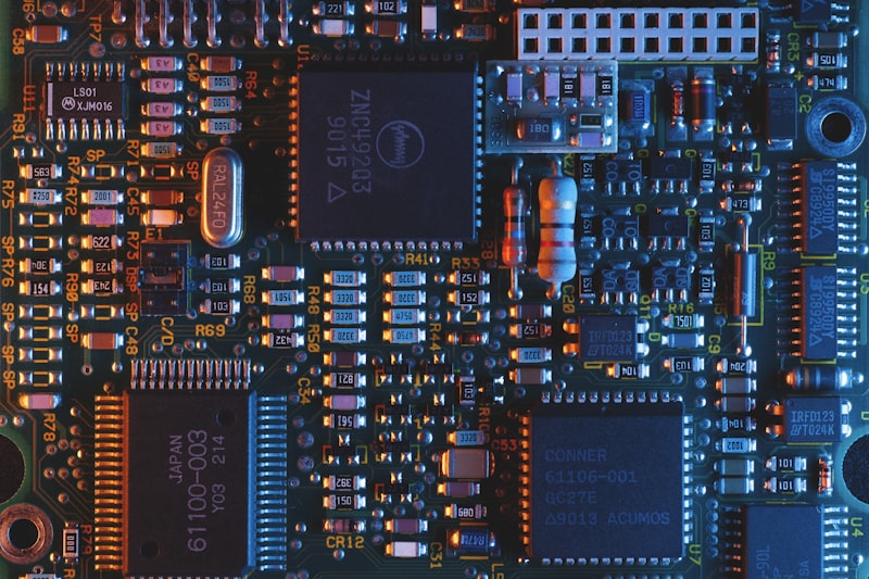
HASL 対 ENIG 対 OSP:直接比較
費用
OSPは、利用可能な表面処理の中で最も安価です。HASL(特にLF-HASL)は中価格帯に位置します。ENIGは、金含有量と多段階の化学処理工程のため、最も高価です。コストが最優先される大量生産の民生用電子機器では、OSPが標準的な選択肢となることがよくあります。一方、長期保存性と優れたはんだ付け性が最優先される医療、航空宇宙、または産業用基板では、ENIGは割高であってもその価値があります。
平面度
OSP and ENIG are both flat finishes suitable for modern fine-pitch assembly. HASL introduces surface variation that can cause co-planarity issues with 0.4 mm pitch BGAs or dense 0201 component layouts. If your design includes QFN packages or micro-BGAs, specify ENIG or OSP—not HASL.
賞味期限と保存方法
HASL offers the best shelf life (12+ months), followed by ENIG (12 months with proper storage), then OSP (6–12 months, with strict handling requirements). For boards that may sit in a warehouse before assembly, HASL or ENIG is the safer choice. OSP boards should be assembled within weeks of opening the vacuum packaging.
RoHS準拠
鉛フリーのHASL、ENIG、およびOSPはいずれもRoHS指令に準拠しています。従来のスズ・鉛系HASLは、EU、英国、またはカリフォルニア州に出荷される民生用電子機器には使用が許可されていません。RoHS対応製品にHASLを施す必要がある場合は、工場側がデフォルトでスズ・鉛系を使用しないよう、必ず「LF-HASL」と指定してください。
表面仕上げに関するIPC規格
IPCは、いくつかの主要な文書において表面仕上げの要件を定めています:
- IPC-4552: ENIG specification — thickness requirements, solderability, adhesion testing
- 相互接続サブアセンブリの組立工程: イマージョン・シルバー(ImAg)の仕様
- 相互接続サブアセンブリの組立工程: OSP specification — film thickness, thermal degradation testing
- J-STD-003: Solderability tests for printed boards — wetting balance and spread tests
PCB製造仕様書を作成する際は、必ず該当するIPC文書と受入クラスを明記してください。これにより、製造工場には明確な品質基準が示され、貴社には不適合な基板を拒否する権利が与えられます。この点を理解することは、 IPCクラス2とクラス3の違い これらは、これらの仕上げ仕様を理解する上で不可欠な背景情報です。
また、以下の点も考慮してください。 医療用および自動車用プリント基板に関する特殊な要件, そこでは、表面仕上げの選定は、IPC規格だけでなく、ISO 13485やIATF 16949といった業界固有の認証基準にも準拠していなければなりません。
適切なPCB表面処理の選び方:ステップバイステップ
ステップ 1:コンポーネントの種類とピッチを定義する
List every package type in your BOM and identify the minimum pad pitch. If you have any 0.4 mm pitch BGA, 0.5 mm pitch QFN, or 0201 passives, planarity is critical—eliminate HASL. Your shortlist becomes OSP or ENIG.
ステップ2:保存期間の要件を評価する
基板の製造から組立までの予想される期間を把握してください。基板が倉庫で6か月以上保管される場合は、OSPの採用はリスクが高くなります。その場合は、HASLまたはENIGを選択してください。基板が製造後数週間以内にJIT組立ラインへ直接搬送される場合は、OSPの採用が可能です。
ステップ3:RoHSおよび規制要件の確認
最終製品がRoHS、REACH、またはその他の規制の対象となるかどうかを確認してください。対象となる場合は、スズ・鉛HASLの使用を中止してください。RoHSの適用除外が認められる軍事用、宇宙用、または高信頼性製品の場合、スズ・鉛HASLの使用が許容されるほか、そのはんだ接合部の信頼性が確立されていることから、むしろ推奨される場合もあります。
ステップ4:リフローサイクルの評価
組立工程におけるリフローおよびウェーブはんだ付けの回数を数えてください。選択的ウェーブはんだ付けを行う両面SMT基板の場合、3回以上の加熱サイクルが必要になることがあります。HASLは複数回のリフローに十分耐えますが、OSPは耐えられません。ENIGは複数回のリフローに耐えますが、最初のサイクルで金が溶解すると、はんだ接合部の品質が変化します。
ステップ5:特別な組み立て要件の評価
Does your design include wire bonding, press-fit connectors, or gold edge fingers? Wire bonding requires ENIG or hard gold (ENEPIG). Press-fit connectors need a consistent, hard metallic surface—ENIG is typical. Edge fingers require hard gold over nickel, specified separately from the board’s main finish.
ステップ6:候補に挙げた仕上げ材の見積もりを取りましょう
Request pricing for your top two options. The cost delta between ENIG and OSP can be $0.10–$0.50 per board depending on board size and complexity. At high volumes, this is significant. At low volumes, the reliability and handling advantages of ENIG often outweigh the cost. Work with your PCBサプライヤーの受注ワークフロー to confirm lead time implications—some finishes add one to two days to cycle time.
よくある質問
PCBの表面処理で最も一般的なものは何ですか?
ENIGは、その平坦性、保存期間、およびRoHS準拠性から高く評価されており、世界的に見て民生用電子機器において最も一般的に指定される表面処理です。HASL(鉛含有および鉛フリーの両方)は、コスト重視の分野、特にアジア太平洋地域の製造現場において依然として主流となっています。OSPは、大量生産かつ短サイクルなJIT組立ラインを運営する大手OEM各社で広く採用されています。
ENIGはHASLよりも優れているのでしょうか?
It depends on the application. ENIG is superior for fine-pitch components, consistent planarity, and wire bonding. HASL is superior for cost-sensitivity, long shelf life, and multiple reflow cycles. Neither is universally better—the right choice is determined by your design’s component pitch, storage requirements, and budget.
ENIGにおいて、ブラックパッドが発生する原因は何ですか?
Black pad is caused by hyper-corrosion of the nickel layer during the immersion gold plating step. Phosphorus-rich grain boundaries in the nickel deposit are preferentially attacked, creating a brittle, oxide-rich interface between the nickel and the solder. The root cause is typically poor bath chemistry control—phosphorus content outside the 6–8% spec range—at the PCB factory. Always request cross-section coupons and ENIG chemistry audit records from your supplier.
OSPはどのくらいの期間続くのですか?
OSP shelf life is typically 6–12 months from the date of manufacture when stored in sealed vacuum packaging at 15–30°C and below 70% relative humidity. Once opened, boards should be assembled within 24–72 hours to minimize oxidation risk. Shelf life degrades faster at elevated temperatures or high humidity, common in tropical climates.
1枚の基板上で、表面処理を組み合わせることはできますか?
Yes, selective finishes are possible. For example, a board may use ENIG on BGA pads and gold edge fingers on connector tabs, with OSP on through-hole pad areas. Selective finish adds cost and complexity but is sometimes justified for mixed-technology boards. Discuss the requirements with your factory during the DFM review stage—typically covered when you PCBメーカーをお選びください.
表面仕上げは、インピーダンス制御基板に影響を与えますか?
表面仕上げは導体の表面粗さに影響を与えますが、ほとんどのデジタル信号において、体積インピーダンスの計算にはほとんど影響しません。しかし、RFおよびマイクロ波周波数(数GHz以上)では、表皮深さが表面粗さの大きさに近づくため、表面粗さが重要な要素となります。RF基板の場合、ENIGやOSPはHASLよりも好まれます。これは、これらの表面仕上げの方が滑らかであるため、導体の損失を低減できるからです。
医療用PCBにはどのような表面処理が最適でしょうか?
医療機器用PCBでは、長期保存性、優れたはんだ付け性の安定性、およびISO 13485に準拠したトレーサビリティ要件から、通常ENIGが指定されます。一部の埋め込み型または高信頼性が求められる医療用途では、ワイヤボンディングとの相性を高めるため、ENEPIG(無電解ニッケル・無電解パラジウム・浸漬金)が使用されます。以下の内容をご確認ください。 医療用プリント基板に関する特別な要件 仕上げの仕様を確定する前に。
PCB工場の監査を行う際、表面仕上げの品質をどのように確認すればよいでしょうか?
工場監査の際には、以下の資料の提出を求めてください:ENIG浴の化学組成記録(ニッケル・リン含有量、金浴のpH、補充記録)、J-STD-003に準拠したはんだ付け性試験用試験片、ENIG層の厚さとニッケルの形態を示す断面レポート、およびOSP膜厚の工程管理図。当社の詳細なガイドについては、 PCBサプライヤーの監査 確認すべき品質チェックポイントの全項目を網羅しています。

結論
PCBの表面処理の選定は、組立歩留まり、実使用時の信頼性、および製品の総コストに直接影響を及ぼす、精密な技術的判断です。HASLは、実証済みのはんだ付け性と長い保存期間を最低コストで実現するため、スルーホールが主流でコスト重視の設計に最適です。ENIGは、ファインピッチ、高密度、および混合技術の基板に求められる平面性と信頼性を提供しますが、そのコストは組立歩留まりの向上によって十分に正当化されることがよくあります。OSPは、基板が長期保管されることなく製造工場から組立ラインへと迅速に搬送される大量生産のJITラインにおいて、最も平坦性が高く、環境に優しい選択肢となります。
The best surface finish for your board is the one that matches your design’s component geometry, assembly process, storage conditions, regulatory requirements, and cost targets. By understanding the trade-offs outlined in this guide, you can specify your surface finish with confidence—and have an informed conversation with your PCB工場またはサプライヤー どのオプションがお客様の生産ニーズに最も適しているかについて。