メタルコア基板
(MCPCB/アルミニウム)
Aluminum-base and copper-base metal core boards engineered to move heat away from the junction — where standard FR4 thermal resistance becomes the limiting factor in your design.
A heat-spreading substrate — not just a circuit board
メタルコアPCBでは、標準的なFR4コアに代わって、固体アルミニウムまたは銅のベースプレートが使用されており、これは熱伝導性誘電体層を介して銅の回路層に接合されています。部品接合部で発生した熱は、この誘電体層を通って垂直方向に金属ベースへと伝導され、そこで横方向に広がってヒートシンクや筐体へと放熱されます。
The dielectric layer is the critical engineering variable. Standard FR4 has a thermal conductivity around 0.3 W/m·K; MCPCB dielectrics range from 1.0 W/m·K for cost-sensitive designs up to 3.0 W/m·K for standard high-power LED work, and up to 8.0 W/m·K for ceramic-filled dielectrics used in the most thermally demanding power modules.
母材の選定も重要です。アルミニウム5052および6061は、コストと加工性の点で、LEDや一般的な電源用途において主流となっています。一方、最大の熱拡散性やより高い機械的強度が求められる場合は、熱性能とコスト面で割高になるものの、銅系材料が指定されます。
Get MCPCB Quote →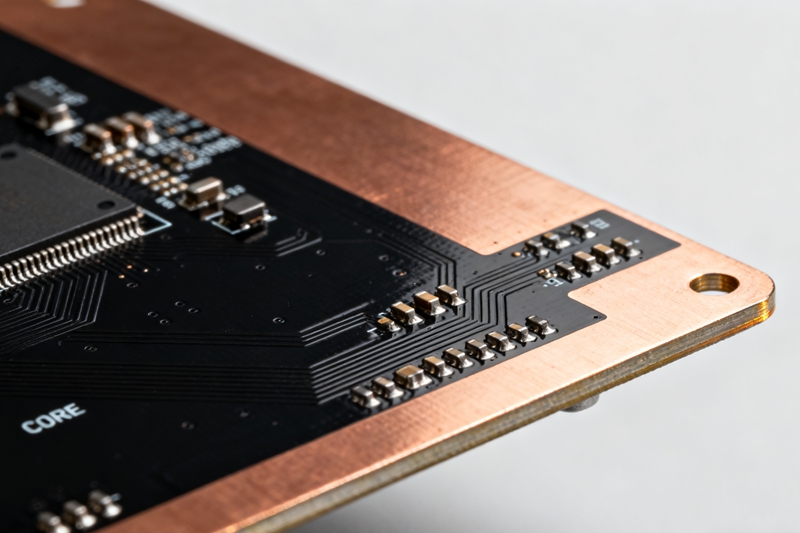
MCPCBの熱性能を左右する3つの仕様決定事項
The datasheet thermal conductivity number is only the starting point — the full construction determines what actually reaches the heatsink.
誘電体層の厚さは、絶縁性と熱伝導経路とのトレードオフである
The dielectric layer sits between the copper circuit and the metal base, providing electrical isolation while conducting heat vertically. Thinner dielectric (75 µm) reduces thermal resistance but limits breakdown voltage; thicker dielectric (150 µm) raises breakdown voltage margin but increases thermal resistance. We specify dielectric thickness against your required breakdown voltage and junction temperature target — not a single default.
75–150 µm dielectric · 1.0–8.0 W/m·K · IPC-2S1B constructions非鉄金属の選定:アルミニウム対銅
アルミニウム5052-H32および6061-T6は、標準的なLED基板や電源基板において、優れた熱拡散性、低コスト、そしてCNCルーター加工の容易さを兼ね備えています。銅ベースは、同じ厚さの場合、アルミニウムの約2倍の熱伝導率を発揮し、誘電体を通じた垂直方向の熱伝導だけでなく、基板の端部への横方向の熱拡散がボトルネックとなる高出力モジュールに採用されています。
Al 5052/6061 · Cu base · 0.8–3.2mm thickness · thermal spreading耐 breakdown 電圧定格が安全マージンを決定する
Per IPC standard test methods, breakdown voltage of the dielectric layer typically ranges 3kV to 4.5kV depending on thickness and filler composition. For LED drivers and power supplies operating from mains-derived rails, breakdown voltage rating must be reviewed against creepage and clearance requirements — a board that meets UL 796 recognition on the dielectric material alone is not automatically safety-compliant at the finished-board level.
UL 796 recognized · 3–4.5kV breakdown · dielectric withstand testフルメタルコア基板の製造仕様
すべての誘電特性および熱特性に関するデータは、サプライヤーのデータシートと照合して検証されており、すべての生産ロットにおいて誘電耐力試験によって確認されています。
加工パラメータ
| 非貴金属 | Aluminum 5052 / 6061 · Copper |
| ベースの厚さ | 0.8 mm – 3.2 mm |
| 誘電体の厚さ | 75 µm – 150 µm |
| 銅の重量 | 1 oz – 10 oz |
| 建設 | Single-layer · Double-layer · Multilayer MCPCB |
性能と基準
| 誘電熱伝導率 | 1.0 – 3.0 W/m·K standard · up to 8.0 W/m·K advanced |
| 耐電圧 | 3kV – 4.5kV |
| 表面仕上げ | HASL-lead-free · ENIG · OSP · White/Black Solder Mask |
| 安全表彰 | UL 796 絶縁体の認定を取得 |
| プロトタイプの納期 | 72h express · 6 days standard |
メタルコア基板の製造方法
A bonding-critical process — the dielectric-to-metal interface determines thermal and mechanical reliability for the life of the board.
ベースプレートの準備と回路のイメージング
アルミニウムまたは銅製のベースプレートに表面処理を施し、銅箔を熱伝導性誘電体と積層した後、フォトリソグラフィーを用いて回路パターンを形成する。
エッチングおよび誘電体ボンディング
銅は最終回路形状にエッチングされ、熱界面の空隙を排除するため、制御された熱と圧力下で誘電体層を介して金属基板上に熱圧着される。
CNCルーター加工・穴あけ加工
機械的な輪郭加工および穴あけは、金属基板の硬度に合わせた超硬工具を用いて行われ、誘電体のエッジ部分での剥離を防ぎます。
ソルダーマスク、表面処理および誘電体試験
ソルダーマスク、表面処理、およびレジェンドの印字を施した後、出荷前に絶縁耐電圧試験を100%実施し、耐電圧定格を確認します。
メタルコア基板が最適な選択肢となる場合
故障モードが電気的ではなく熱的な設計は、すべてメタルコア構造の適用候補となります。
LED街路灯・周辺照明
屋外で、持続的に高い周囲温度下で動作する高出力LED照明器具向けの、アルミニウム基板を用いた単層MCPCB。
自動車用照明
自動車用途の全範囲にわたって安定した接合部温度が求められる、高CCT LEDを搭載したヘッドランプおよびDRLモジュール。
電源装置およびコンバータ
パワーMOSFETからシャーシへの直接的な熱伝達経路が必要な、スイッチングレギュレータおよびAC/DCコンバータ基板向けのMCPCB。
モーター駆動装置
コンパクトな筐体内で連続的なスイッチング損失を放散する、モータードライバ段用の銅基板MCPCB。
D級オーディオアンプ
低熱抵抗が求められるクラスDアンプモジュールにおける出力段MOSFET用のアルミニウム基板。
耐熱性自動車用電子機器
ボンネット下やエンジン付近に設置される電子モジュールで、部品のディレーティングマージンが効果的な放熱に依存するもの。
産業用パワーモジュール
産業用ドライブおよび再生可能エネルギー用インバータにおけるIGBTおよびパワーモジュールキャリア用の多層MCPCB。
太陽光およびUV硬化アレイ
パネル全体に均一な熱分布が求められる、UV硬化および園芸用照明向けの高密度LEDアレイ。
MCPCB quality — from dielectric selection to breakdown voltage test.
メタルコア基板の品質は、誘電体の適格性評価から始まります。当社のDFMレビューでは、お客様の消費電力値に基づいて熱経路の計算を確認します。製造後、100%の誘電耐力試験を実施し、すべての基板について絶縁破壊電圧を確認します。
- ISO 9001:2015第三者による監査を受けた品質管理
- 国際PCB規格リジッドPCBの認定および性能
- IPC-A-600 クラス 2 / 3許容基準
- UL 796誘電体材料の安全性に関する認定
- RoHS / REACHEUの有害物質規制への準拠
検査および試験方法
- 100% Electrical Test — Flying Probe / Fixtureすべてのネットにおいて、ロング/ショート
- 100% 絶縁耐電圧試験Confirms 3kV–4.5kV breakdown rating per lot
- 熱抵抗の検証Measured against dielectric datasheet W/m·K value
- 100% AOI — Circuit Layer自動光学検査
- Peel Strength — Copper to DielectricIPC-TM-650 2.4.8 に準拠した接合部の完全性
- ソルダーマスクの密着性および膜厚クロスハッチ試験および厚さ測定試験
- 熱衝撃サイクル試験-40°C to +125°C on request
- 寸法/CNC輪郭検証図面との照合による配管後の測定
当社が製造したメタルコア基板
Real thermal management challenges — solved.
200W LED街路灯の熱設計の見直し
Migrated from 1.0 W/m·K dielectric aluminum board to 3.0 W/m·K construction after field reports of premature LED lumen depreciation in high-ambient regions.
Junction temperature reduced by 18°C at rated drive current. L70 lumen maintenance life projection improved from 35,000h to 60,000h.
500W AC/DCコンバータ用銅基板MCPCB
ヒートシンクに取り付けられたFR4製ドーターカードに代わる、2層構造の銅基板MCPCB。これにより、熱伝導経路がパワーステージ基板に直接統合されています。
独立したヒートシンクアセンブリを排除したことで、筐体の容積を22%削減しつつ、全負荷時においてもMOSFETのケース温度をディレーティング仕様の範囲内に抑えることに成功した。
自動車用DRLモジュール用アルミニウムMCPCB
1.2mm aluminum-base single-layer board for daytime running light module, qualified across -40°C to +105°C automotive ambient range.
500サイクルの熱衝撃試験に合格し、誘電体と銅の界面で剥離は一切発生しませんでした。2年間にわたり量産されています。
メタルコアPCBに関するよくある質問
MCPCBの熱設計、材料、製造に関する技術的な質問。
For general LED lighting and moderate power applications, 1.0–2.0 W/m·K dielectric is typically sufficient and cost-effective. For high-power LED (street lighting, high-bay), power converters and motor drives, 3.0 W/m·K is the common standard. For the most thermally demanding power module and high-density LED array designs, ceramic-filled dielectrics up to 8.0 W/m·K are available. We recommend a thermal review of your power dissipation and target junction temperature before finalizing dielectric selection.
Aluminum 5052 or 6061 is the default choice for most LED and general power applications — good thermal spreading, lower cost, and easier CNC routing. Copper base delivers roughly double the thermal conductivity of aluminum at equivalent thickness and is worth the cost premium when lateral heat spreading across the board (not just vertical conduction through the dielectric) is the limiting factor, such as in high-power modules with concentrated heat sources.
はい。単層MCPCB(金属基板上に1層の回路が形成されたもの)は、最も一般的で低コストな構造であり、LEDアプリケーションの大部分で使用されています。2層および多層MCPCB構造では、基板の上に追加の回路層が配置され、メッキスルーホールまたはビアによって接続されています。これらは、LEDアレイと同じ基板上にドライバ回路を統合する場合など、単層では対応できないほど高い配線密度が設計上必要となる場合に使用されます。
標準的なMCPCBの絶縁破壊電圧は、厚さや充填材の組成に応じて3kVから4.5kVの範囲となります。商用電源由来の電圧を扱う基板については、最終製品の安全規格(例:IEC 62368-1)で要求される沿面距離および空間距離とともに、絶縁破壊電圧の定格を確認する必要があります。絶縁体の厚さと耐電圧定格が適切に整合するよう、DFMレビューの際に、安全認証の目標を当社のエンジニアリングチームにお知らせいただくことをお勧めします。
We support copper weights from 1 oz up to 10 oz on MCPCB circuit layers. Heavier copper (4 oz and above) is common in power supply and motor drive MCPCB designs to increase current-carrying capacity of the traces alongside the thermal path through the dielectric. Heavier copper requires wider minimum trace/space due to etch factor — this is reviewed during DFM.
Yes. 100% of MCPCB production is tested for dielectric withstand voltage before shipment, confirming the board meets the specified breakdown voltage rating (3kV–4.5kV depending on construction). Test results are included in the quality documentation package supplied with each order, alongside the material Certificate of Compliance for the dielectric layer.
Get your MCPCB thermal design reviewed — today.
ガーバーデータ、電力損失値、および目標接合部温度をお送りください。当社のエンジニアが、8時間以内に誘電体の選定、ベースメタル、および絶縁破壊電圧について検討いたします。
- すべてのお問い合わせには、DFMおよび熱設計のレビューが含まれます
- NDA signed on request — standard practice
- 8営業時間以内にご返信いたします
- 72時間での迅速な試作が可能
- お見積もりのご依頼に、ご契約の義務は一切ありません
お見積りのお申し込み
以下の詳細をご記入ください。折り返しご連絡いたします。