메탈 코어 PCB
(MCPCB / 알루미늄)
Aluminum-base and copper-base metal core boards engineered to move heat away from the junction — where standard FR4 thermal resistance becomes the limiting factor in your design.
A heat-spreading substrate — not just a circuit board
금속 코어 PCB는 표준 FR4 코어 대신 고체 알루미늄 또는 구리 베이스 플레이트를 사용하며, 이 베이스 플레이트는 열전도성 유전체 층을 통해 구리 회로층에 접합됩니다. 소자 접합부에서 발생하는 열은 이 유전체 층을 통해 수직으로 금속 베이스로 전달되며, 그곳에서 열은 방열판이나 섀시로 측면으로 확산됩니다.
The dielectric layer is the critical engineering variable. Standard FR4 has a thermal conductivity around 0.3 W/m·K; MCPCB dielectrics range from 1.0 W/m·K for cost-sensitive designs up to 3.0 W/m·K for standard high-power LED work, and up to 8.0 W/m·K for ceramic-filled dielectrics used in the most thermally demanding power modules.
기판 금속의 선택도 중요합니다. 알루미늄 5052와 6061은 비용과 가공성 측면에서 LED 및 일반 전력 응용 분야에서 주로 사용됩니다. 반면, 최대의 열 확산 성능이나 더 높은 기계적 강도가 요구되는 경우에는 열 성능과 비용 면에서 더 높은 수준이 필요하지만 구리 기판이 지정됩니다.
Get MCPCB Quote →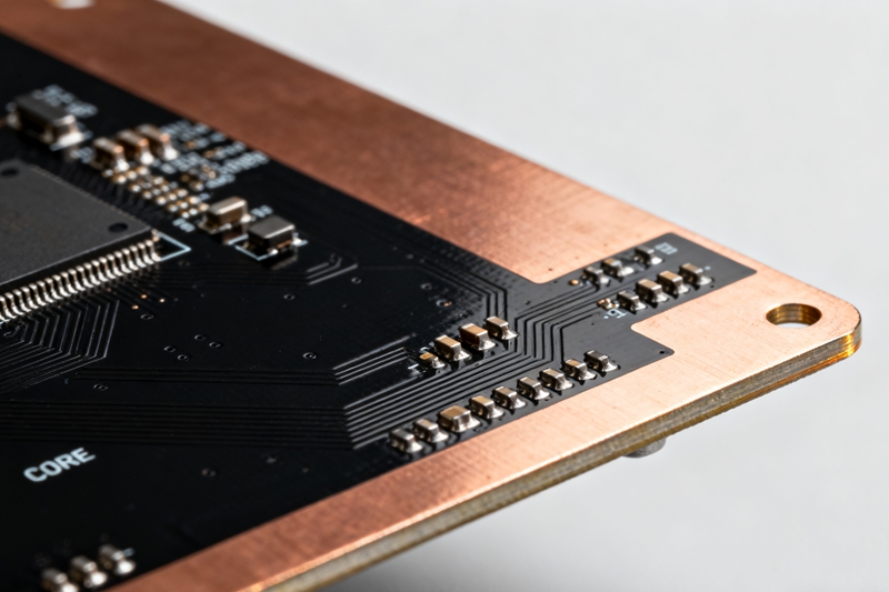
MCPCB의 열 성능을 결정하는 세 가지 사양 결정 사항
The datasheet thermal conductivity number is only the starting point — the full construction determines what actually reaches the heatsink.
유전체 층의 두께는 절연성과 열 전달 경로 간의 절충점이다
The dielectric layer sits between the copper circuit and the metal base, providing electrical isolation while conducting heat vertically. Thinner dielectric (75 µm) reduces thermal resistance but limits breakdown voltage; thicker dielectric (150 µm) raises breakdown voltage margin but increases thermal resistance. We specify dielectric thickness against your required breakdown voltage and junction temperature target — not a single default.
75–150 µm dielectric · 1.0–8.0 W/m·K · IPC-2S1B constructions비철금속 선택: 알루미늄 대 구리
알루미늄 5052-H32 및 6061-T6은 표준 LED 및 전원 공급 장치 기판에 대해 우수한 열 확산 성능, 저렴한 비용, 그리고 손쉬운 CNC 라우팅 가공을 제공합니다. 구리 베이스는 동일한 두께에서 알루미늄보다 약 2배 높은 열전도율을 제공하며, 유전체를 통한 수직 전도뿐만 아니라 기판 가장자리로의 횡방향 열 확산이 병목 현상이 되는 고출력 모듈에 사용하도록 지정되어 있습니다.
Al 5052/6061 · Cu base · 0.8–3.2mm thickness · thermal spreading정격 파단 전압이 안전 여유를 결정합니다
Per IPC standard test methods, breakdown voltage of the dielectric layer typically ranges 3kV to 4.5kV depending on thickness and filler composition. For LED drivers and power supplies operating from mains-derived rails, breakdown voltage rating must be reviewed against creepage and clearance requirements — a board that meets UL 796 recognition on the dielectric material alone is not automatically safety-compliant at the finished-board level.
UL 796 recognized · 3–4.5kV breakdown · dielectric withstand test풀 메탈 코어 PCB 제작 사양
모든 유전 및 열 관련 데이터는 공급업체의 데이터시트를 기준으로 검증되었으며, 모든 생산 로트에 대해 유전 내압 시험을 통해 확인되었습니다.
가공 매개변수
| 비귀금속 | Aluminum 5052 / 6061 · Copper |
| 베이스 두께 | 0.8 mm – 3.2 mm |
| 유전체 두께 | 75 µm – 150 µm |
| 구리 무게 | 1 oz – 10 oz |
| 건설 | Single-layer · Double-layer · Multilayer MCPCB |
성능 및 표준
| 유전체 열전도도 | 1.0 – 3.0 W/m·K standard · up to 8.0 W/m·K advanced |
| 파괴 전압 | 3kV – 4.5kV |
| 표면 마감 | HASL-lead-free · ENIG · OSP · White/Black Solder Mask |
| 안전 표창 | UL 796 절연체 인증 획득 |
| 시제품 제작 기간 | 72h express · 6 days standard |
메탈 코어 PCB의 제조 과정
A bonding-critical process — the dielectric-to-metal interface determines thermal and mechanical reliability for the life of the board.
베이스 플레이트 준비 및 회로 이미징
알루미늄 또는 구리 베이스 플레이트에 표면 처리를 하고, 구리 포일을 열전도성 유전체와 적층한 다음, 포토리소그래피 공정을 통해 회로 패턴을 형성합니다.
에칭 및 유전체 본딩
구리는 최종 회로 모양으로 식각된 후, 제어된 열과 압력 하에서 유전체 층을 통해 금속 기판에 열압착되어 열 접합면의 공극을 제거합니다.
CNC 라우팅 및 드릴링
금속 기판의 경도에 맞춘 초경 공구를 사용하여 기계적 윤곽 라우팅 및 구멍 뚫기 공정을 수행함으로써, 유전체 가장자리에서 발생하는 박리 현상을 방지합니다.
솔더 마스크, 표면 처리 및 유전체 시험
솔더 마스크, 표면 마감 및 레전드를 적용한 후, 출하 전에 절연 내전압 등급을 확인하기 위해 100% 절연 내전압 시험을 실시합니다.
메탈 코어 PCB가 적합한 경우
고장 원인이 전기적 요인이 아닌 열적 요인인 모든 설계는 금속 코어 구조의 적용 대상이 됩니다.
LED 가로등 및 지역 조명
지속적으로 높은 주변 온도 조건에서 실외에서 작동하는 고출력 LED 조명 기구용 알루미늄 기반 단층 MCPCB.
자동차 조명
자동차용 전 범위에서 안정적인 접합 온도가 요구되는 고-CCT LED가 탑재된 헤드램프 및 DRL 모듈.
전원 공급 장치 및 변환기
전력 MOSFET이 섀시와 직접적인 열 전달 경로를 필요로 하는 스위칭 레귤레이터 및 AC/DC 컨버터 보드용 MCPCB.
모터 구동 장치
소형 인클로저 내에서 연속 스위칭 손실을 방출하는 모터 드라이버 스테이지용 구리 기반 MCPCB.
D급 오디오 증폭기
열 저항이 낮은 것이 요구되는 클래스 D 증폭기 모듈의 출력단 MOSFET용 알루미늄 기판.
열에 민감한 자동차 전자 부품
부품의 정격 감축 여유가 효과적인 열 확산에 좌우되는 엔진 후드 내부 및 엔진 인근의 전자 모듈.
산업용 전원 모듈
산업용 드라이브 및 재생에너지 인버터에 사용되는 IGBT 및 전력 모듈 캐리어용 다층 MCPCB.
태양광 및 자외선 경화 어레이
패널 전체에 걸쳐 균일한 열 분포가 필요한 자외선 경화 및 원예용 조명을 위한 고밀도 LED 어레이.
MCPCB quality — from dielectric selection to breakdown voltage test.
메탈 코어 기판의 품질은 유전체 재료의 적합성 평가에서 시작됩니다. 당사의 DFM 검토 과정에서는 고객의 전력 손실 수치에 맞춰 열 경로 계산을 확인합니다. 제조 후 진행되는 100% 유전체 내전압 테스트를 통해 모든 기판의 절연 파괴 전압을 확인합니다.
- ISO 9001:2015제3자 감사를 거친 품질 관리
- 국제 PCB 표준경질 PCB의 인증 및 성능
- IPC-A-600 등급 2 / 3수용 기준
- UL 796유전체 재료의 안전성 인정
- RoHS / REACHEU 유해 물질 규정 준수
검사 및 시험 방법
- 100% Electrical Test — Flying Probe / Fixture모든 네트에서 매수/매도 포지션
- 100% 유전 내전압 시험Confirms 3kV–4.5kV breakdown rating per lot
- 열 저항 검증Measured against dielectric datasheet W/m·K value
- 100% AOI — Circuit Layer자동 광학 검사
- Peel Strength — Copper to DielectricIPC-TM-650 2.4.8에 따른 접합 무결성
- 솔더 마스크의 접착력 및 두께교차 선 그리기 및 두께 측정 시험
- 열충격 사이클링-40°C to +125°C on request
- 치수 / CNC 윤곽 검증도면을 기준으로 한 라우팅 후 측정
당사가 제작한 금속 코어 기판
Real thermal management challenges — solved.
200W LED 가로등 열 설계 재설계
Migrated from 1.0 W/m·K dielectric aluminum board to 3.0 W/m·K construction after field reports of premature LED lumen depreciation in high-ambient regions.
Junction temperature reduced by 18°C at rated drive current. L70 lumen maintenance life projection improved from 35,000h to 60,000h.
500W AC/DC 변환기 구리 기판 MCPCB
방열판에 장착된 FR4 도터 카드를 대체하는 2층 구리 기판 기반 MCPCB로, 열 전달 경로를 전원 스테이지 보드에 직접 통합합니다.
별도의 방열판 어셈블리를 제거함으로써, 최대 부하 시에도 MOSFET 케이스 온도를 정격 저하 사양 범위 내로 유지하면서 인클로저 부피를 22% 줄였습니다.
자동차용 DRL 모듈 알루미늄 MCPCB
1.2mm aluminum-base single-layer board for daytime running light module, qualified across -40°C to +105°C automotive ambient range.
500사이클 열충격 시험을 통과했으며, 유전체와 구리 사이의 계면에서 박리 현상이 전혀 발생하지 않았습니다. 2년 동안 양산 중입니다.
메탈 코어 PCB에 관한 자주 묻는 질문
MCPCB의 열 설계, 소재 및 제조와 관련된 기술적 질문.
For general LED lighting and moderate power applications, 1.0–2.0 W/m·K dielectric is typically sufficient and cost-effective. For high-power LED (street lighting, high-bay), power converters and motor drives, 3.0 W/m·K is the common standard. For the most thermally demanding power module and high-density LED array designs, ceramic-filled dielectrics up to 8.0 W/m·K are available. We recommend a thermal review of your power dissipation and target junction temperature before finalizing dielectric selection.
Aluminum 5052 or 6061 is the default choice for most LED and general power applications — good thermal spreading, lower cost, and easier CNC routing. Copper base delivers roughly double the thermal conductivity of aluminum at equivalent thickness and is worth the cost premium when lateral heat spreading across the board (not just vertical conduction through the dielectric) is the limiting factor, such as in high-power modules with concentrated heat sources.
네. 단층 MCPCB(금속 기판 위에 회로층이 하나 있는 구조)는 가장 일반적이고 비용이 가장 저렴한 구조로, 대부분의 LED 응용 분야에 사용됩니다. 이중층 및 다층 MCPCB 구조는 기판 위에 추가적인 회로층을 배치하고, 도금 관통공(plated through-holes) 또는 비아(vias)로 연결한 것으로, LED 어레이와 동일한 기판에 드라이버 회로가 통합되는 경우처럼 단층 구조로는 지원하기 어려운 높은 배선 밀도가 필요한 설계에 사용됩니다.
표준 MCPCB의 유전체 절연 파괴 전압은 두께와 충전재 구성에 따라 3kV에서 4.5kV 사이입니다. 주전원 전압을 처리하는 기판의 경우, 최종 제품 안전 표준(예: IEC 62368-1)에서 요구하는 크리프 거리 및 청간 거리와 함께 절연 파괴 전압 등급을 검토해야 합니다. 유전체 두께와 전압 정격이 올바르게 설정될 수 있도록, DFM 검토 과정에서 귀사의 안전 인증 목표를 당사 엔지니어링 팀에 알려주시기를 권장합니다.
We support copper weights from 1 oz up to 10 oz on MCPCB circuit layers. Heavier copper (4 oz and above) is common in power supply and motor drive MCPCB designs to increase current-carrying capacity of the traces alongside the thermal path through the dielectric. Heavier copper requires wider minimum trace/space due to etch factor — this is reviewed during DFM.
Yes. 100% of MCPCB production is tested for dielectric withstand voltage before shipment, confirming the board meets the specified breakdown voltage rating (3kV–4.5kV depending on construction). Test results are included in the quality documentation package supplied with each order, alongside the material Certificate of Compliance for the dielectric layer.
Get your MCPCB thermal design reviewed — today.
Gerber 파일, 전력 손실 수치 및 목표 접합 온도를 보내 주십시오. 당사 엔지니어들이 8시간 이내에 유전체 선정, 베이스 금속 및 항복 전압을 검토해 드립니다.
- 모든 문의 건에 DFM 및 열 설계 검토가 포함됩니다
- NDA signed on request — standard practice
- 영업일 기준 8시간 이내 답변
- 72시간 내 제작 가능한 신속 시제품 제공
- 견적 요청 시 별도의 약정이 필요하지 않습니다
견적 요청하기
아래에 세부 정보를 입력해 주시면 곧 연락드리겠습니다.