경질 PCB
(다층)
From 2-layer prototypes to 32-layer high-speed server boards — the foundation of every electronic system, built to the specification your design actually demands.
The workhorse board technology — built correctly for your application
경질 다층 PCB는 구리 피복 라미네이트(코어)와 접착 프리프레그 층을 쌓아 올린 후, 열과 압력을 가해 압착하여 하나의 경질 기판으로 형성한 것입니다. 스루홀 비아와 블라인드 비아는 회로 설계에 따라 각 층을 연결합니다.
The word 'standard' is misleading. Material selection, stackup design and fabrication process control vary enormously between suppliers — and these variables directly determine signal performance, thermal reliability and service life.
From standard FR4 for office electronics to high-Tg polyimide for engine bay automotive boards and Rogers laminates for RF designs — the right specification starts with a DFM review that checks the stackup, not just the DRC.
Get Rigid PCB Quote →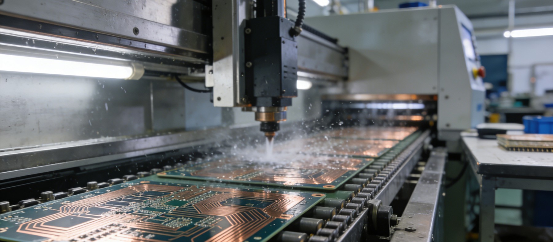
경질 PCB의 성능을 좌우하는 세 가지 사양 결정 사항
서로 다른 적층 구조로 제작된 동일한 회로도는 성능이 달라집니다. 이것이 가장 중요한 변수들입니다.
Stackup Design Controls Impedance — and Impedance Controls Signal Quality
Every high-speed trace on a PCB is a transmission line. Its characteristic impedance is set by trace width, dielectric thickness and laminate Dk — variables that are chosen in the stackup design step, before fabrication begins. A stackup that isn't reviewed against your signal speed targets will produce a board that doesn't perform to simulation, every time.
controlled impedance · Dk vs frequency · TDR verification · ±5% tolerance온도, 습도 및 화학적 환경에 따른 재료 선정
Standard FR4 handles office temperatures and moderate humidity adequately. Automotive engine bay boards at continuous 125°C need high-Tg FR4 (Tg 170–220°C) or polyimide. Outdoor industrial boards exposed to condensation require low-water-absorption laminates. Specifying the wrong base material is the most common root cause of premature PCB failure in the field.
high-Tg FR4 · polyimide · low-water-absorption · halogen-free options구리 배럴의 두께가 장기적인 신뢰성을 좌우한다
A board that passes electrical test on day one can still fail after 500 thermal cycles if via copper barrel thickness is marginal. IPC-6012 specifies minimum copper thickness in via barrels (18 µm minimum average). Only microsection analysis can confirm this was achieved. We include microsection analysis on every production lot — not as an extra charge, but as a baseline quality requirement.
IPC-6012 via barrel · 18 µm min Cu · microsection QC · thermal cycle life완전 경질 PCB 제작 사양
모든 공정 매개변수는 당사의 ISO 9001 품질경영시스템(QMS)을 통해 검증됩니다. 임피던스가 제어된 모든 주문품에는 TDR 임피던스 보고서가 함께 제공됩니다.
가공 매개변수
| 레이어 수 | 2 – 32 layers |
| 최소 트레이스 / 스페이스 | 2.5 / 2.5 밀 |
| 최소 구멍 크기 | 0.20 mm mechanical · 0.10 mm laser |
| 구리 무게 | 0.5 oz – 20 oz |
| 판 두께 | 0.4 mm – 6.4 mm |
성능 및 표준
| 제어 임피던스 | ±5% TDR verified |
| 라미네이트 옵션 | FR4 · High-Tg · Polyimide · Rogers · Halogen-free |
| 표면 마감 | HASL · ENIG · ENEPIG · OSP · Immersion Ag |
| IPC 조립 표준 | Class 2 default · Class 3 on request |
| 시제품 제작 기간 | 48h express · 5 days standard |
다층 PCB의 제조 과정
More process steps than most electronic manufacturing — each one affecting the final board's reliability.
내층 이미징 및 식각
구리 피복 라미네이트는 포토리소그래피 공정을 통해 이미지가 형성되고, 최종 내부층 회로 패턴이 드러날 때까지 식각됩니다. 산화 처리를 통해 적층을 위한 표면이 준비됩니다.
스택업 프레스
Inner cores, prepreg and copper foils are precisely aligned and hot-pressed at 175–220°C under 350 psi. Resin flow fills all voids and bonds layers permanently.
드릴링 및 디스미어
스루홀은 초경 비트를 사용하여 CNC 가공으로 뚫습니다. 플라즈마 데스미어 공정을 통해 비아 벽면의 에폭시 수지를 제거하여 구리가 내부 레이어 패드에 확실히 접착되도록 합니다.
도금, 이미징 및 마감
IPC-6012 규격에 따라 비전해 및 전해 구리 도금을 기판 벽면에 적용합니다. 외층 이미징, ENIG/OSP 마감 처리 및 전기적 테스트를 거쳐 공정이 완료됩니다.
경질 다층 PCB가 적합한 경우
Standard rigid multilayer is the foundation of virtually every electronic product — the specification is what varies.
산업용 컨트롤러 및 PLC
고온 환경에서 사용되는 PLC, 모션 컨트롤러 및 산업용 컴퓨터용 고 Tg 다층 필름.
서버 및 네트워킹
DDR5, PCIe 5.0 및 400G 이더넷을 지원하는 서버용 CPU, 스위치 ASIC 및 라인 카드용 고층수 기판.
자동차 ECU
자동차의 전체 온도 범위에서 엔진 제어, 차체 제어 및 ADAS 처리를 위한 고신뢰성 다층 회로.
의료 기기
영상 시스템, 환자 모니터 및 수술 장비용 IPC Class 3 다층 기판.
전력 전자공학
고전류 버스바가 장착된 모터 구동 장치, 전력 변환기 및 UPS 시스템용 고두께 구리 다층 기판.
통신 인프라
DSLAM, OLT 및 라우팅 장비용 상위 계층 백플레인 및 라인 카드 기판.
가전제품
스마트 TV, 셋톱박스 및 가전제품용 비용 효율적인 다층 구조.
방위 전자기기
광범위한 온도 범위와 IPC Class 3 규격을 충족해야 하는 군용 전자기기용 폴리이미드 다층 기판.
Rigid PCB quality — from stackup review to via barrel verification.
경질 PCB의 품질 관리는 제조 단계 이전부터 시작됩니다. 당사의 DFM 검토를 통해 구리 식각 공정이 시작되기 전에 적층 구조 및 소재 관련 문제를 사전에 파악합니다. 제조 후에는 100% 전기적 테스트와 선택적 미세 단면 분석을 통해 모든 로트의 비아 배럴 품질을 확인합니다.
- ISO 9001:2015제3자 감사를 거친 품질 관리
- 국제 PCB 표준경질 PCB의 인증 및 성능
- IPC-A-600 등급 2 / 3수용 기준
- RoHS / REACHEU 유해 물질 규정 준수
검사 및 시험 방법
- 100% Electrical Test — Flying Probe / Fixture모든 네트에서 매수/매도 포지션
- 100% AOI — All Layers자동 광학 검사
- Impedance Test — TDR±5% verified per production lot
- 미세단면 및 단면 분석IPC-6012에 따른 배럴 도금 구리 두께
- 굽히기와 비틀기IPC-TM-650 2.4.22
- 박리 강도IPC-TM-650 2.4.8에 따른 구리 접착력
- 열 응력 플로트 시험288°C solder float per IPC-TM-650 2.6.8
- 이온 크로마토그래피요청 시 이온 청정도
당사에서 제작한 경질 보드
Real multilayer fabrication challenges — solved.
16층 고 Tg 산업용 PLC 기판
Tg 180°C laminate, ±5% impedance on Ethernet and fieldbus, IPC Class 3, operating in a steel plant at continuous 85°C ambient.
Passed 1,000-cycle thermal shock -40°C to +85°C. Zero PCB-related field failures in 5 years of steel plant deployment.
28층 데이터 센터 스위치 보드
PCIe 5.0, DDR5-6400 and 400GbE signals, back-drilled via stubs, Isola I-Tera low-Dk laminate, ±5% impedance on all high-speed lines.
PCIe 5.0 아이 다이어그램이 사양을 18%의 여유로 충족했습니다. 첫 시도에서 NEBS 레벨 3 인증을 통과했습니다.
12층 자동차용 BCM
High-Tg FR4, -40°C to +125°C, IPC Class 2, IATF 16949 documentation package, conformal coating-compatible stackup.
FAI는 첫 제출 시 승인되었습니다. 3년간의 생산 기간 동안 PCB로 인한 현장 반품 건수는 단 한 건도 없었습니다.
경질 다층 PCB에 관한 자주 묻는 질문
다층 PCB 제조, 소재 및 품질에 관한 기술적 질문.
Our standard controlled impedance tolerance is ±5%, verified by TDR measurement and reported with each order. Tighter tolerances of ±3% are available on request for applications such as test and measurement instruments or ultra-high-speed server boards — these require tighter trace width control (±0.5 mil) and low-Dk variance laminates such as Isola I-Tera or Rogers 4350B.
We stock and process: high-Tg FR4 (Tg 150°C / 170°C / 180°C), polyimide (Tg 260°C+), halogen-free FR4, Rogers 4350B / RO4003C for RF applications, Isola I-Tera MT40 for high-speed digital, and specialty low-Dk laminates for demanding signal integrity requirements. Laminate selection is reviewed during the DFM process and material CoC is supplied with each order.
표준 순차적 제작 방식의 경질 다층 회로 기판의 경우, 최대 레이어 수는 32층입니다. 20층을 초과하는 제작의 경우, 견적 요청 단계에서 당사 엔지니어링 팀에 문의하여 제작 전략, 스택업 옵션 및 리드 타임에 미치는 영향에 대해 논의하시기 바랍니다. 블라인드 비아 및 매립 비아 설계는 최대 30층까지 지원됩니다.
당사의 기계식 드릴링 최소 구멍 직경은 0.20 mm이며, 최대 종횡비(기판 두께 : 구멍 직경)는 12:1입니다. 더 작은 구멍의 경우, 레이저 드릴링을 통해 0.10 mm 직경을 구현할 수 있습니다. 높은 종횡비의 관통 구멍이 필요한 기판(예: 두께 3.2 mm 이상에 비아 직경이 작은 경우)의 경우, 주문하기 전에 당사 엔지니어링 팀에 문의하여 적층 구조 검토를 받으시기 바랍니다.
We offer copper weights from 0.5 oz (17 µm) for fine-line HDI inner layers to 20 oz (700 µm) for heavy copper power bus boards. Standard options are 1 oz and 2 oz on outer layers, 0.5 oz and 1 oz on inner layers. Heavy copper designs (>3 oz) require special handling in the etching and imaging process and are quoted with extended lead time.
Via barrel copper thickness is verified by microsection analysis — physical cross-section of representative vias from each production lot. The minimum copper thickness in via barrels is 18 µm per IPC-6012 Class B/C requirements. Microsection reports showing average, minimum and maximum barrel copper readings are included in our quality documentation package for each lot.
Get your rigid PCB stackup reviewed — today.
Gerber 파일과 스택업 사양을 보내주십시오. 당사의 엔지니어들이 8시간 이내에 임피던스 목표치, 소재 선정 및 비아 종횡비를 검토해 드립니다.
- 모든 문의 시 DFM 검토가 포함됩니다
- NDA signed on request — standard practice
- 영업일 기준 8시간 이내 답변
- 48시간 내 시제품 제작 가능
- 견적 요청 시 별도의 약정이 필요하지 않습니다
견적 요청하기
아래에 세부 정보를 입력해 주시면 곧 연락드리겠습니다.