リジッド基板
(多層)
From 2-layer prototypes to 32-layer high-speed server boards — the foundation of every electronic system, built to the specification your design actually demands.
The workhorse board technology — built correctly for your application
リジッド多層PCBは、銅張積層板(コア)と接着性プリプレグ層を積み重ね、熱と圧力をかけて圧着し、単一のリジッド基板を形成したものです。回路設計の要件に応じて、スルービアおよびブラインドビアによって各層が接続されます。
The word 'standard' is misleading. Material selection, stackup design and fabrication process control vary enormously between suppliers — and these variables directly determine signal performance, thermal reliability and service life.
From standard FR4 for office electronics to high-Tg polyimide for engine bay automotive boards and Rogers laminates for RF designs — the right specification starts with a DFM review that checks the stackup, not just the DRC.
Get Rigid PCB Quote →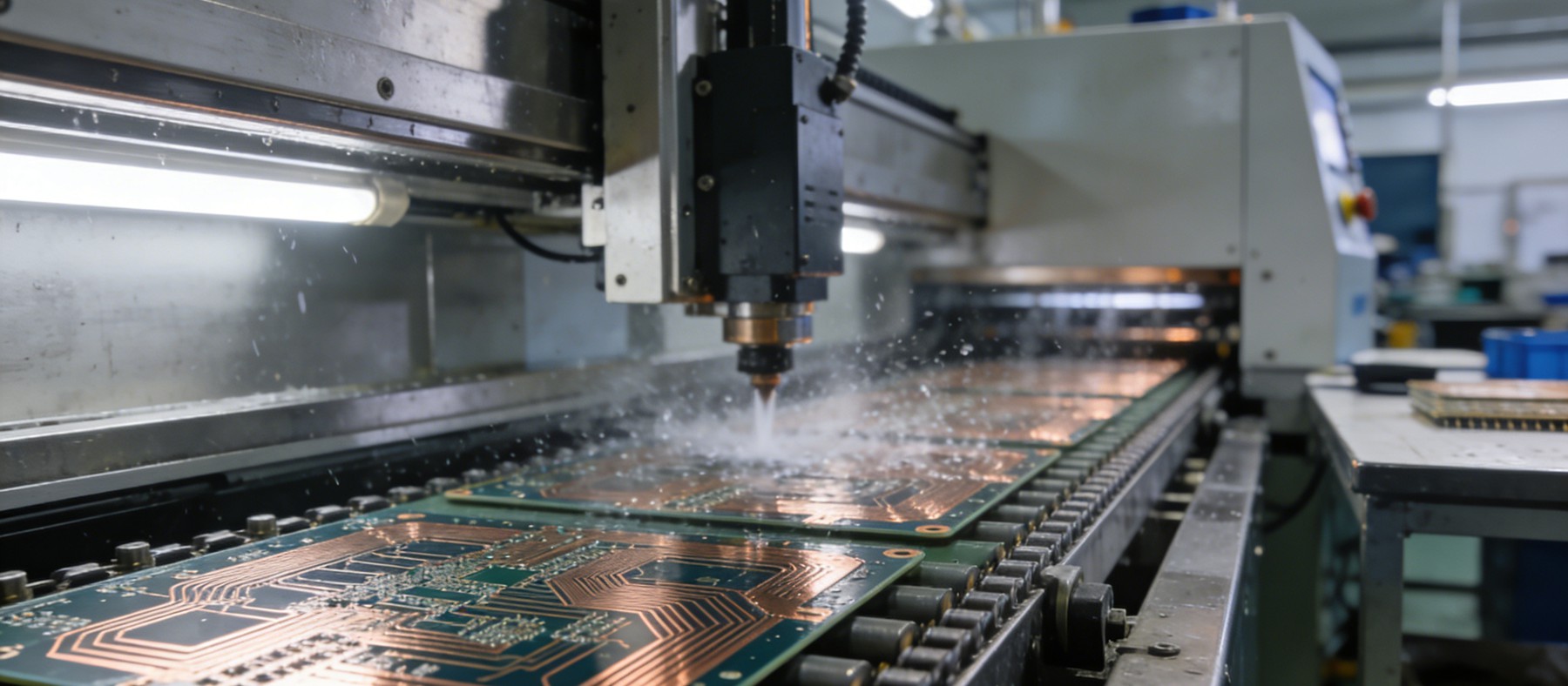
リジッドPCBの性能を左右する3つの仕様決定事項
異なる積層構造で作成された2つの同一の回路図では、その動作特性が異なります。これらが最も重要な変数となります。
Stackup Design Controls Impedance — and Impedance Controls Signal Quality
Every high-speed trace on a PCB is a transmission line. Its characteristic impedance is set by trace width, dielectric thickness and laminate Dk — variables that are chosen in the stackup design step, before fabrication begins. A stackup that isn't reviewed against your signal speed targets will produce a board that doesn't perform to simulation, every time.
controlled impedance · Dk vs frequency · TDR verification · ±5% tolerance温度、湿度、および化学的環境に応じた材料選定
Standard FR4 handles office temperatures and moderate humidity adequately. Automotive engine bay boards at continuous 125°C need high-Tg FR4 (Tg 170–220°C) or polyimide. Outdoor industrial boards exposed to condensation require low-water-absorption laminates. Specifying the wrong base material is the most common root cause of premature PCB failure in the field.
high-Tg FR4 · polyimide · low-water-absorption · halogen-free optionsCopper Barrelによると、バレルの厚さが長期的な信頼性を左右する
A board that passes electrical test on day one can still fail after 500 thermal cycles if via copper barrel thickness is marginal. IPC-6012 specifies minimum copper thickness in via barrels (18 µm minimum average). Only microsection analysis can confirm this was achieved. We include microsection analysis on every production lot — not as an extra charge, but as a baseline quality requirement.
IPC-6012 via barrel · 18 µm min Cu · microsection QC · thermal cycle lifeフルリジッドPCBの製造仕様書
すべてのプロセスパラメータは、当社のISO 9001品質マネジメントシステム(QMS)を通じて検証されています。インピーダンス制御製品のご注文には、すべてTDRインピーダンスレポートが添付されます。
加工パラメータ
| 層数 | 2 – 32 layers |
| 最小トレース/スペース | 2.5 / 2.5 ミル |
| 最小穴径 | 0.20 mm mechanical · 0.10 mm laser |
| 銅の重量 | 0.5 oz – 20 oz |
| ボードの厚さ | 0.4 mm – 6.4 mm |
性能と基準
| 制御インピーダンス | ±5% TDR verified |
| ラミネートの種類 | FR4 · High-Tg · Polyimide · Rogers · Halogen-free |
| 表面仕上げ | HASL · ENIG · ENEPIG · OSP · Immersion Ag |
| IPC構築基準 | Class 2 default · Class 3 on request |
| プロトタイプの納期 | 48h express · 5 days standard |
多層プリント基板の製造工程
More process steps than most electronic manufacturing — each one affecting the final board's reliability.
内層のイメージングおよびエッチング
銅張積層板は、フォトリソグラフィーにより露光・エッチングされ、最終的な内層回路パターンが形成されます。酸化処理により、積層のための表面が整えられます。
スタックアッププレス
Inner cores, prepreg and copper foils are precisely aligned and hot-pressed at 175–220°C under 350 psi. Resin flow fills all voids and bonds layers permanently.
ドリリングおよびデスミア
スルーホールは、超硬ビットを用いてCNC加工で穿孔されます。プラズマ脱脂処理により、ビアの壁面からエポキシ樹脂を除去し、内層のパッドへの銅の密着を確保します。
メッキ、画像処理、仕上げ
IPC-6012規格に準拠し、壁面に対して無電解銅めっき、続いて電解銅めっきを施します。外層のパターン形成、ENIG/OSP仕上げ、および電気的試験を経て、プロセスが完了します。
リジッド多層PCBが最適な選択肢となる場合
Standard rigid multilayer is the foundation of virtually every electronic product — the specification is what varies.
産業用コントローラおよびPLC
高温環境下で使用されるPLC、モーションコントローラ、および産業用コンピュータ向けの、高Tg多層フィルム。
サーバー・ネットワーク
DDR5、PCIe 5.0、400Gイーサネットを搭載した、サーバー用CPU、スイッチ用ASIC、およびラインカード向けの多層基板。
自動車用ECU
自動車の全温度範囲にわたって、エンジン制御、ボディ制御、およびADAS処理に対応する高信頼性の多層フィルム。
医療機器
画像診断システム、患者モニター、および手術用機器向けのIPCクラス3多層基板。
パワーエレクトロニクス
大電流バスバーを備えたモーター駆動装置、電力変換装置、およびUPSシステム向けの厚銅多層基板。
通信インフラ
DSLAM、OLT、およびルーティング機器向けのハイレイヤー・バックプレーンおよびラインカード基板。
家電製品
スマートテレビ、セットトップボックス、家電製品向けのコスト効率に優れた多層フィルム。
防衛用電子機器
広範囲の温度条件およびIPCクラス3が要求される軍事用電子機器向けのポリイミド多層基板。
Rigid PCB quality — from stackup review to via barrel verification.
リジッドPCBの品質確保は、製造工程が始まる前から始まります。当社のDFMレビューでは、銅のエッチングが行われる前に、積層構成や材料に関する問題を発見します。製造後、100%の電気的検査と選択的な微細断面検査により、すべてのロットにおいてビアバレルの品質を確認しています。
- ISO 9001:2015第三者による監査を受けた品質管理
- 国際PCB規格リジッドPCBの認定および性能
- IPC-A-600 クラス 2 / 3許容基準
- RoHS / REACHEUの有害物質規制への準拠
検査および試験方法
- 100% Electrical Test — Flying Probe / Fixtureすべてのネットにおいて、ロング/ショート
- 100% AOI — All Layers自動光学検査
- Impedance Test — TDR±5% verified per production lot
- マイクロセクションおよび断面解析IPC-6012に基づくバレルめっき銅の厚さ
- お辞儀とひねりIPC-TM-650 2.4.22
- 剥離強度IPC-TM-650 2.4.8 に準拠した銅の密着性
- 熱応力フロート試験288°C solder float per IPC-TM-650 2.6.8
- イオンクロマトグラフィーご要望に応じたイオン清浄度
当社が製作したリジッド基板
Real multilayer fabrication challenges — solved.
16層・高Tg工業用PLC基板
Tg 180°C laminate, ±5% impedance on Ethernet and fieldbus, IPC Class 3, operating in a steel plant at continuous 85°C ambient.
Passed 1,000-cycle thermal shock -40°C to +85°C. Zero PCB-related field failures in 5 years of steel plant deployment.
28層データセンター用スイッチボード
PCIe 5.0, DDR5-6400 and 400GbE signals, back-drilled via stubs, Isola I-Tera low-Dk laminate, ±5% impedance on all high-speed lines.
PCIe 5.0のアイダイアグラムは、18%のマージンを確保して仕様を満たしました。NEBSレベル3の認定を初回で取得しました。
12層構造の自動車用BCM
High-Tg FR4, -40°C to +125°C, IPC Class 2, IATF 16949 documentation package, conformal coating-compatible stackup.
FAIは初回提出で承認されました。生産開始から3年間、PCBに起因するフィールドリターンはゼロでした。
リジッド多層PCBに関するよくある質問
多層プリント基板の製造、材料、品質に関する技術的な質問。
Our standard controlled impedance tolerance is ±5%, verified by TDR measurement and reported with each order. Tighter tolerances of ±3% are available on request for applications such as test and measurement instruments or ultra-high-speed server boards — these require tighter trace width control (±0.5 mil) and low-Dk variance laminates such as Isola I-Tera or Rogers 4350B.
We stock and process: high-Tg FR4 (Tg 150°C / 170°C / 180°C), polyimide (Tg 260°C+), halogen-free FR4, Rogers 4350B / RO4003C for RF applications, Isola I-Tera MT40 for high-speed digital, and specialty low-Dk laminates for demanding signal integrity requirements. Laminate selection is reviewed during the DFM process and material CoC is supplied with each order.
標準的な順次積層方式によるリジッド多層基板の最大層数は32層です。20層を超える基板については、お見積り依頼の段階で当社のエンジニアリングチームにご連絡いただき、製造戦略、積層構成の選択肢、およびリードタイムへの影響についてご相談いただくことをお勧めします。ブラインドビアおよび埋込ビアの設計は、最大30層まで対応可能です。
当社の機械加工による穴あけの最小径は0.20 mmで、最大アスペクト比(基板厚さ:穴径)は12:1です。これより小さい穴については、レーザー加工により0.10 mmの径を実現しています。高いアスペクト比のスルーホールが必要な基板(例:厚さ3.2 mm以上でビア径が小さい場合)については、ご注文の前に当社のエンジニアリングチームまでご連絡いただき、積層構成の確認を行ってください。
We offer copper weights from 0.5 oz (17 µm) for fine-line HDI inner layers to 20 oz (700 µm) for heavy copper power bus boards. Standard options are 1 oz and 2 oz on outer layers, 0.5 oz and 1 oz on inner layers. Heavy copper designs (>3 oz) require special handling in the etching and imaging process and are quoted with extended lead time.
Via barrel copper thickness is verified by microsection analysis — physical cross-section of representative vias from each production lot. The minimum copper thickness in via barrels is 18 µm per IPC-6012 Class B/C requirements. Microsection reports showing average, minimum and maximum barrel copper readings are included in our quality documentation package for each lot.
Get your rigid PCB stackup reviewed — today.
ガーバーデータおよび積層仕様をお送りください。当社のエンジニアが、8時間以内にインピーダンス目標値、材料選定、ビアのアスペクト比について確認いたします。
- すべてのお問い合わせにDFMレビューが含まれます
- NDA signed on request — standard practice
- 8営業時間以内にご返信いたします
- 48時間でのプロトタイプ作成が可能
- お見積もりのご依頼に、ご契約の義務は一切ありません
お見積りのお申し込み
以下の詳細をご記入ください。折り返しご連絡いたします。