現代のエレクトロニクス業界において、小型化は最優先事項です。消費者の期待が、より小型・軽量で高性能な電子機器へとシフトするにつれ、高効率なプリント基板(PCB)レイアウトへの需要は飛躍的に高まっています。このスペース効率への絶え間ない追求こそが、高密度配線(HDI)基板とブラインドビア技術が活躍の場となる理由です。ブラインドビアは、基板を完全に貫通させることなく、基板の外層と内層を戦略的に接続することで、重要な配線スペースを確保します。これにより、電気エンジニアは、極めて限られた設置面積の中に、はるかに多くの機能、部品、および配線を詰め込むことが可能になります。正確に理解することは スマートデバイスがコンパクトな設計を実現するためにHDI基板の積層構造を必要とする理由 これは、ブラインドビア技術がもたらすレイアウトの真の可能性を十分に理解するための第一歩となります。
ブラインドビア技術とは何ですか?
A blind via is a specialized type of interconnection used in multi-layer printed circuit boards. It connects the top or bottom outer layer of the PCB to one or more immediately adjacent inner layers but deliberately stops short of penetrating the entire thickness of the board. Because it is only visible and accessible from one side of the board—referred to as the “blind” side—it leaves the opposite exterior surface completely intact and untouched. This pristine area on the opposite side can subsequently be used for placing additional surface mount technology (SMT) components, or it can be utilized for routing more complex traces, dramatically increasing the board’s overall component and routing density.
これとは対照的に、標準的なスルーホールビアは、回路基板を上面から下面まで貫通しています。製造はより簡単ですが、スルーホールビアは、電気的な接続が実際に必要とされない層であっても、内部層および外部層のすべてにおいて貴重な基板面積を大幅に消費してしまいます。特に、スペースに制約のある高度な設計を扱う場合、ブラインドビア技術の導入は極めて重要です。例えば、 10層のPCB積層構造による複雑な電源要件への対応、スルーホールビアの使用を最小限に抑えることは、連続した堅牢な電源プレーンおよびグランドプレーンの構造的および電気的完全性を維持するために絶対に不可欠です。
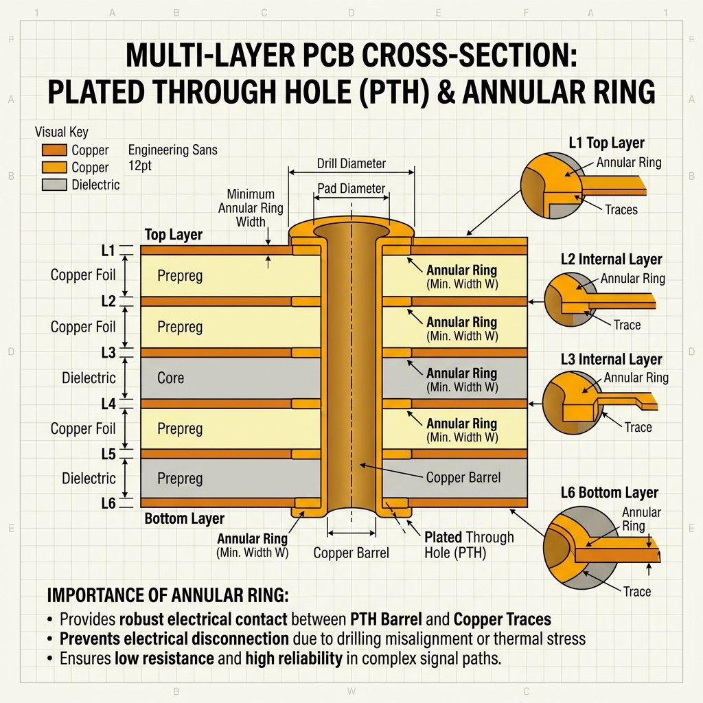
PCB設計におけるブラインドビアの実装方法
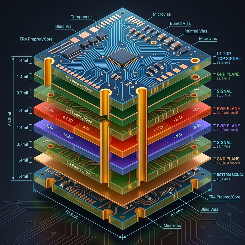
ブラインドビアを用いた設計のための戦略的アプローチ
これらの体系的な手順に従うことで、ブラインドビア技術を活用した、信頼性が高く、製造性に優れたHDI基板の設計が可能になります。
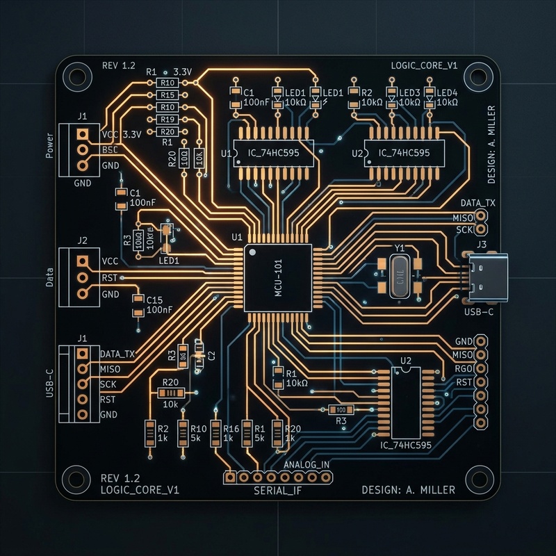
ブラインドビア技術がもたらす変革的なメリット
The primary and most immediately apparent advantage of employing blind via technology is the massive, transformative increase in available board real estate. By completely freeing up segments of different layers, designers are empowered to achieve significantly shorter signal paths. These shorter paths inherently improve signal integrity and simultaneously reduce harmful electromagnetic interference (EMI). Furthermore, utilizing fewer through-hole vias mathematically translates to fewer impedance discontinuities along critical signal paths, which is an absolutely vital consideration for modern high-speed digital designs. While blind vias do undeniably add complexity and a premium cost to the bare board manufacturing process—typically requiring advanced sequential lamination cycles or precision laser drilling—the spatial trade-off is almost always necessary and well worth it for producing cutting-edge smart devices, wearable tech, and sophisticated medical instrumentation.