In the modern era of electronics, miniaturization is paramount. As consumer expectations shift towards smaller, lighter, and more capable electronics, the need for highly efficient printed circuit board (PCB) layouts has grown exponentially. This relentless drive for space efficiency is exactly where high-density interconnect (HDI) boards and blind via technology come into play. By strategically connecting the outer layers of a board to its internal layers without drilling completely through the substrate, blind vias free up crucial routing space. This allows electrical engineers to pack significantly more functionality, components, and traces into a tightly constrained footprint. Understanding exactly why smart devices require an HDI PCB stackup for compact designs is the foundational step toward fully appreciating the raw layout power that blind via technology can unleash.
What is Blind Via Technology?
A blind via is a specialized type of interconnection used in multi-layer printed circuit boards. It connects the top or bottom outer layer of the PCB to one or more immediately adjacent inner layers but deliberately stops short of penetrating the entire thickness of the board. Because it is only visible and accessible from one side of the board—referred to as the “blind” side—it leaves the opposite exterior surface completely intact and untouched. This pristine area on the opposite side can subsequently be used for placing additional surface mount technology (SMT) components, or it can be utilized for routing more complex traces, dramatically increasing the board’s overall component and routing density.
By stark contrast, a standard through-hole via penetrates the entire circuit board from top to bottom. While simpler to manufacture, a through-hole via aggressively consumes valuable real estate on every single internal and external layer, even on those layers where an electrical connection is not actively required. Implementing blind via technology is especially critical when dealing with advanced, space-constrained designs. For instance, when managing complex power requirements with a 10 layer PCB stackup, minimizing the use of through-hole vias is absolutely essential to preserve the structural and electrical integrity of solid, uninterrupted power and ground planes.
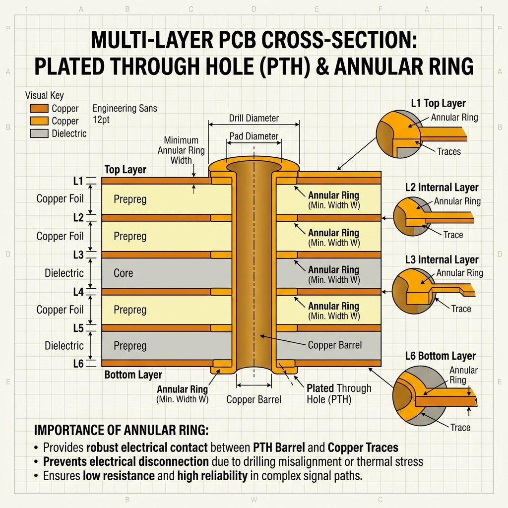
How to Implement Blind Vias in Your PCB Design
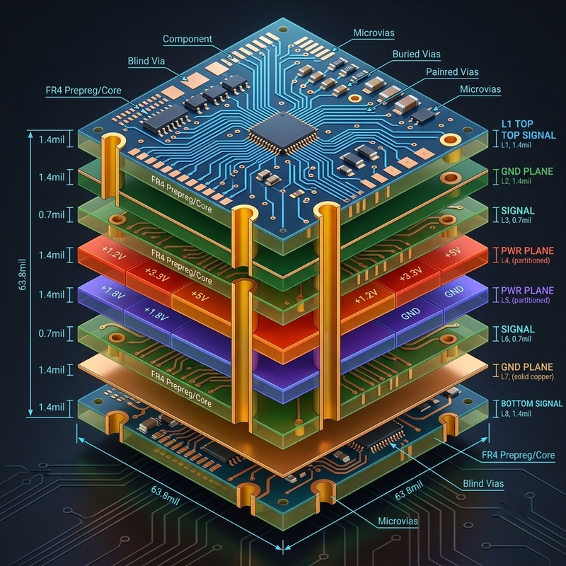
Strategic Steps for Designing with Blind Vias
Following these methodical steps ensures a reliable and highly manufacturable HDI PCB design utilizing blind via technology.
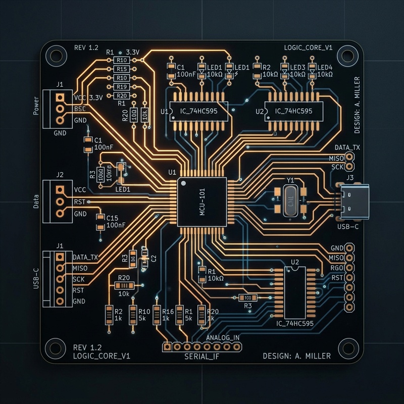
The Transformative Benefits of Blind Via Technology
The primary and most immediately apparent advantage of employing blind via technology is the massive, transformative increase in available board real estate. By completely freeing up segments of different layers, designers are empowered to achieve significantly shorter signal paths. These shorter paths inherently improve signal integrity and simultaneously reduce harmful electromagnetic interference (EMI). Furthermore, utilizing fewer through-hole vias mathematically translates to fewer impedance discontinuities along critical signal paths, which is an absolutely vital consideration for modern high-speed digital designs. While blind vias do undeniably add complexity and a premium cost to the bare board manufacturing process—typically requiring advanced sequential lamination cycles or precision laser drilling—the spatial trade-off is almost always necessary and well worth it for producing cutting-edge smart devices, wearable tech, and sophisticated medical instrumentation.