Introduction
In the realm of Printed Circuit Board (PCB) design and manufacturing, choosing the right method to connect components and layers is a critical decision. While Surface Mount Technology (SMT) has become the dominant method for assembling components onto modern PCBs due to its space-saving and automated assembly advantages, there are specific scenarios where a through hole via connection remains absolutely indispensable. Understanding the strengths of both approaches allows engineers to design robust, reliable, and efficient circuit boards that meet the specific demands of their application.
What is a Through Hole Via?
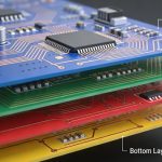
A through hole via is a plated hole in a PCB that connects traces and pads from the top layer to the bottom layer, and potentially to internal layers in a multi-layer board. The hole is typically drilled mechanically and then plated with copper (Plated Through Hole or PTH) to ensure a solid electrical connection. These vias are essential for routing complex signals and providing strong mechanical anchors for larger components that need to endure physical stress.
While SMT relies on pads on the surface of the board, through hole components feature leads that are inserted into these vias and soldered, providing a robust physical bond. For a deeper understanding of proper hole dimensioning, you should review the guide on Выбор подходящего размера отверстий в печатной плате для компонентов со сквозными отверстиями.
When to Use Through Hole Via Connections over SMT
There are several distinct scenarios where incorporating a through hole via is significantly more beneficial than relying solely on Surface Mount Technology:
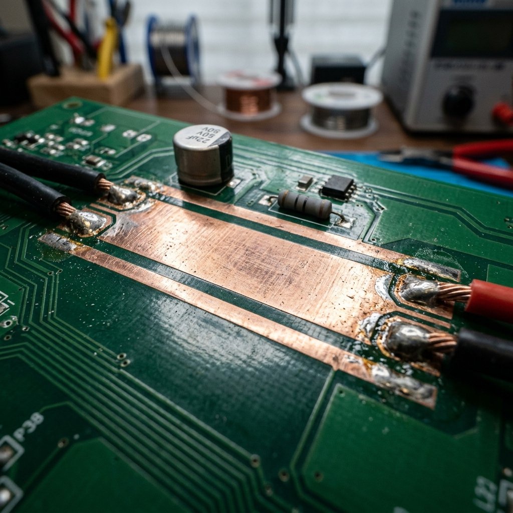
- Mechanical Durability: Connectors, switches, and large relays undergo frequent physical stress. Through hole leads soldered into a plated via provide unmatched mechanical strength compared to surface mount pads which can be ripped off the board under sheer stress.
- High Power Applications: High-current components generate substantial heat and require robust electrical connections. Through hole vias can handle higher currents and dissipate heat more effectively. You can further enhance this by learning Как оптимизировать заливку меди на печатной плате для лучшего отвода тепла.
- Prototyping and Testing: During the initial phases of development, breadboarding and manual soldering are common. Through hole components are much easier to handle, insert, and replace manually than microscopic SMT parts.
- Legacy Components: Some specialized or older components are simply not available in SMT packages, forcing the use of through hole via methods for assembly.
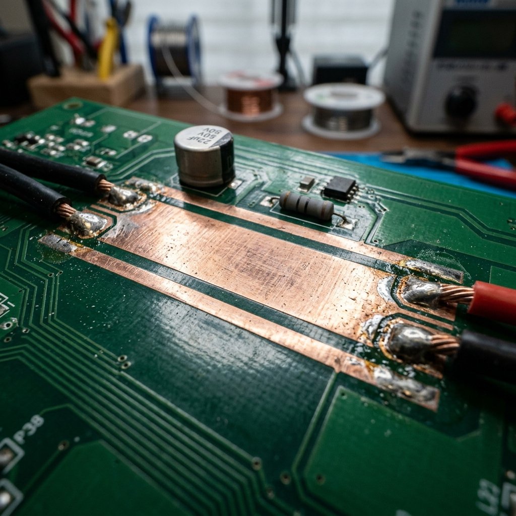
How to Choose Between Through Hole Via and SMT
Follow these steps to determine whether to use through hole vias or surface mount components for your specific PCB design.
Step 1: Evaluate Mechanical Stress Requirements
Identify components that will face user interaction or physical strain, such as I/O connectors or large capacitors. If the mechanical stress is high, select through hole via connections for those specific parts.
Step 2: Assess Power and Thermal Demands
Determine the current ratings and heat dissipation needs. For high-power scenarios, through hole connections combined with large copper planes offer superior performance. However, for efficient SMT placement alongside these, remember to apply Основные рекомендации по проектированию контактных площадок печатных плат для обеспечения надёжной сборки по технологии SMT.
Step 3: Consider Manufacturing and Assembly Costs
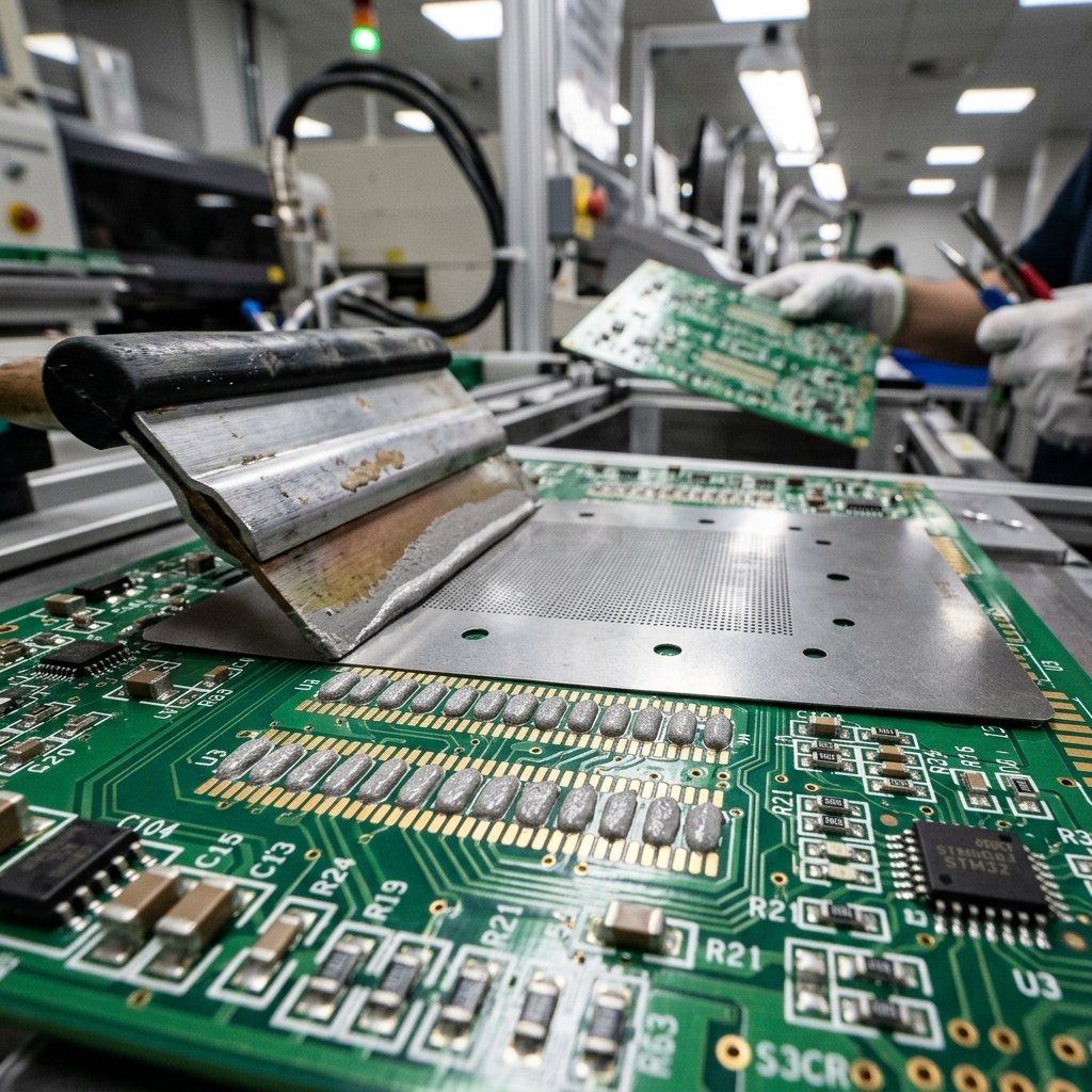
For high-volume production, prioritize SMT to maximize automated pick-and-place efficiency. Limit through hole vias to only those components where SMT falls short, as mixed-technology boards require secondary soldering processes like wave soldering, which increases costs.
Step 4: Review Space Constraints
If board real estate is minimal, SMT is the obvious choice. Through hole vias require more surface area and consume space on all layers of the board, whereas SMT parts only occupy the layer they are mounted on.
Manufacturing Considerations for Vias
When designing PCBs with through hole via connections, manufacturing tolerances must be strictly observed. Adequate spacing and clearance are required to prevent solder bridging during assembly. For example, understanding Почему соблюдение зазоров под паяльной маской на печатной плате важно для пайки без дефектов is crucial to ensuring that the solder flows correctly into the via and does not short adjacent pads.
Часто задаваемые вопросы
Are through hole vias more expensive to manufacture?
Yes, PCBs with a high density of through hole vias can be slightly more expensive due to the mechanical drilling and plating processes required. Additionally, assembling through hole components often requires wave soldering or manual labor, which adds to the final assembly cost compared to fully automated SMT lines.
Can I use both SMT and through hole vias on the same board?
Absolutely. This is called a mixed-technology PCB and is extremely common. Designers often use SMT for microprocessors, memory, and small passive components to save space, while using through hole via connections for connectors, power switches, and large electrolytic capacitors that require structural rigidity.
Does a through hole via affect signal integrity?
In high-speed digital and RF designs, a through hole via can act as a stub and introduce capacitance and inductance, potentially degrading signal integrity. For standard speed and analog applications, however, this effect is usually negligible. For critical high-speed traces, designers often use blind or buried vias instead of standard through hole vias to minimize signal reflection.
Заключение
In conclusion, the decision to use a through hole via connection instead of surface mount technology is dictated by the specific mechanical, thermal, and electrical requirements of the design. While SMT continues to push the boundaries of miniaturization and manufacturing efficiency, the robust, enduring characteristics of through hole vias ensure they will remain a vital tool in the electronics engineer’s arsenal for the foreseeable future. By carefully assessing each component’s role and environmental stressors, designers can leverage the best of both worlds, creating resilient, high-performance printed circuit boards.