In the complex world of printed circuit board (PCB) design and manufacturing, seemingly minor details can have a massive impact on the final product’s reliability and performance. One such critical detail is solder mask clearance. If you are involved in PCB design, fabrication, or assembly, understanding why solder mask clearance matters is absolutely essential for achieving defect-free soldering.
What is Solder Mask Clearance?
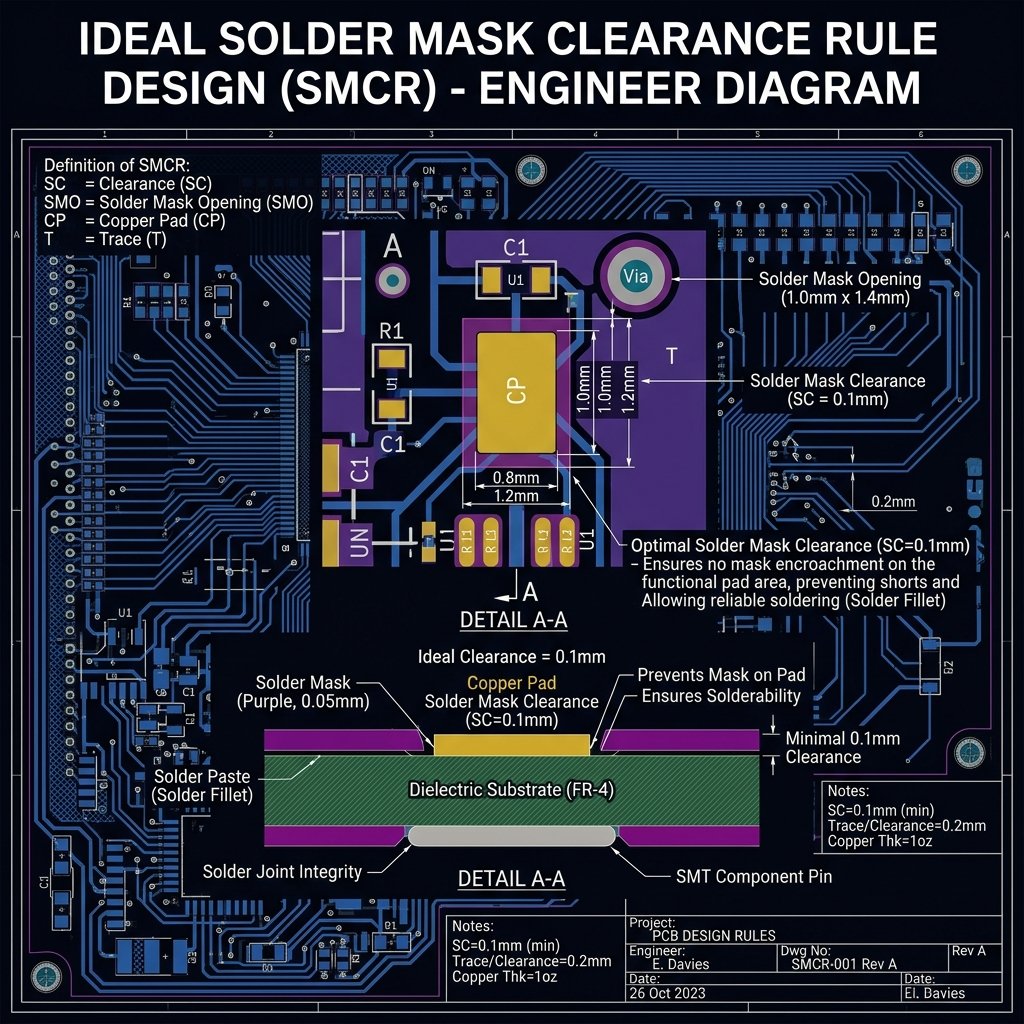
Solder mask, the usually green protective layer on a PCB, prevents solder from bridging between closely spaced pads and traces. Solder mask clearance refers to the intentional gap or opening in the solder mask layer around a copper pad, via, or other exposed metallic features. This clearance ensures that the solder mask does not inadvertently cover any part of the pad that needs to be soldered.

Without adequate clearance, the solder mask can encroach onto the pad. This slight overlap can disrupt the solder paste printing process and the subsequent reflow soldering, leading to a myriad of manufacturing defects. Manufacturers typically recommend a clearance of a few mils (thousandths of an inch) to account for registration tolerances during the solder mask application process.
The Consequences of Improper Clearance
When the solder mask clearance is too small or nonexistent, the likelihood of soldering defects skyrockets. The most common issues include:
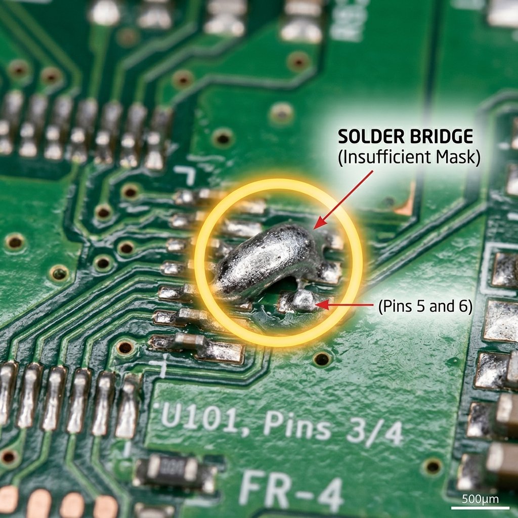
- Solder Bridges: If the mask encroaches on a pad, it can push solder paste outward during reflow, causing it to bridge with an adjacent pad. This creates a short circuit that will render the PCB non-functional.
- Tombstoning: Uneven solder mask coverage on the pads of a two-terminal component (like a resistor or capacitor) can lead to unequal surface tension forces during reflow. This imbalance can cause the component to stand on end, resembling a tombstone.
- Poor Solder Joints: Solder mask on a pad prevents the solder from forming a strong intermetallic bond with the copper. This results in weak joints that are prone to mechanical failure or intermittent electrical connections.
Designing for Optimal Solder Mask Clearance
Achieving defect-free soldering starts at the design phase. PCB designers must adhere to the Design for Manufacturability (DFM) guidelines provided by their chosen fabrication house. These guidelines will specify the minimum solder mask clearance required based on the manufacturer’s equipment capabilities and registration tolerances.
It is crucial to define these clearances accurately in your PCB design software’s design rules. A common rule of thumb is a clearance of 2-3 mils per side, but this can vary depending on the board’s density and the specific manufacturing process (e.g., Liquid Photoimageable solder mask vs. Dry Film). Furthermore, designers must consider the “solder mask web”—the minimum sliver of solder mask that can be reliably manufactured between two adjacent pads.
How to Check Solder Mask Clearance in Your PCB Design
Checking Your Design for Proper Clearance
Follow these steps to ensure your PCB design has adequate solder mask clearance before sending it for fabrication.
1. Review Manufacturer Capabilities
Before setting up your design rules, consult your PCB manufacturer’s capabilities regarding minimum solder mask clearance and minimum solder mask web width.
2. Configure Design Rule Checks (DRC)
Open your PCB layout software and navigate to the Design Rules section. Enter the manufacturer’s specified values for solder mask clearance and web width.
3. Run the DRC Tool
Execute the Design Rule Check across your entire board. The software will highlight any areas where the clearance is less than your specified minimum.
4. Manually Inspect Critical Areas
Even with a DRC pass, it’s wise to manually inspect high-density areas, fine-pitch components, and BGA packages to ensure the clearances are visually correct and the solder mask web is present where necessary.
5. Generate and Verify Gerber Files
After finalizing the layout, generate the Gerber files. Use a Gerber viewer tool to load the top and bottom solder mask layers alongside the copper layers to double-check the clearances one last time before production.
Frequently Asked Questions
What is the difference between solder mask defined (SMD) and non-solder mask defined (NSMD) pads?
In an SMD pad, the solder mask opening is smaller than the copper pad, meaning the solder mask overlaps the pad edges. In an NSMD pad, the solder mask opening is larger than the pad (this is solder mask clearance), leaving a gap between the pad and the mask. NSMD is generally preferred for better solder joint reliability.
Can I have zero solder mask clearance?
Zero solder mask clearance, meaning the mask opening is exactly the same size as the pad, is highly discouraged. Due to manufacturing tolerances, misregistration will almost certainly cause the mask to partially cover the pad, leading to soldering defects.
What happens if the solder mask clearance is too large?
If the clearance is excessively large, it can expose adjacent traces or leave too little solder mask web between closely spaced pads. This increases the risk of solder bridging between a pad and an adjacent trace or between two pads.
Conclusion
Solder mask clearance is a fundamental aspect of PCB design that directly influences manufacturability and product yield. By understanding the critical role it plays in preventing defects like solder bridges and poor joints, designers can create more robust and reliable circuit boards. Always collaborate closely with your manufacturer and leverage DRC tools to ensure your clearances are optimized for success.