The Importance of Thermal Management in PCBs
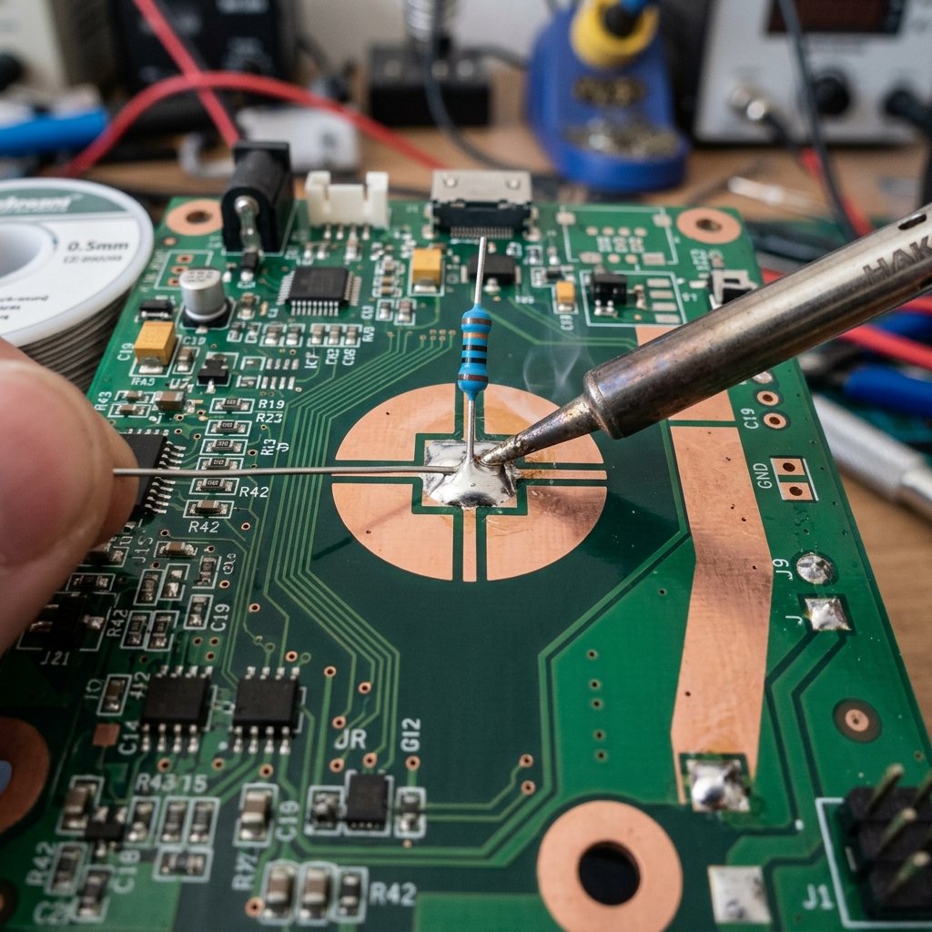
Thermal management is a critical aspect of PCB design. When components are soldered onto a board, whether through wave soldering, reflow soldering, or manual hand soldering, a specific thermal profile must be followed. If a pad connected to a large copper plane lacks a thermal relief connection, the immense thermal mass of the plane will absorb the heat. This requires the assembler or the automated equipment to apply heat for a longer duration, which significantly increases the risk of thermal damage to the PCB substrate (delamination) or the electronic component itself.
Furthermore, in a reflow soldering process, unequal heat distribution can lead to a defect known as “tombstoning,” especially for small, two-terminal surface mount components like resistors and capacitors. Tombstoning occurs when the solder paste on one pad melts before the other, causing surface tension to pull the component upright on the melted end. Proper thermal relief ensures that pads on both ends of a component heat up at a similar rate, drastically reducing the likelihood of this issue.
How to Implement PCB Thermal Relief
Follow these steps to correctly implement thermal relief connections in your PCB design software.
Step 1: Identify Pads Connected to Copper Planes
Review your schematic and PCB layout to identify all component pads, vias, and through-holes that are electrically connected to large copper planes (e.g., ground and power planes).
Step 2: Configure Global Thermal Relief Rules
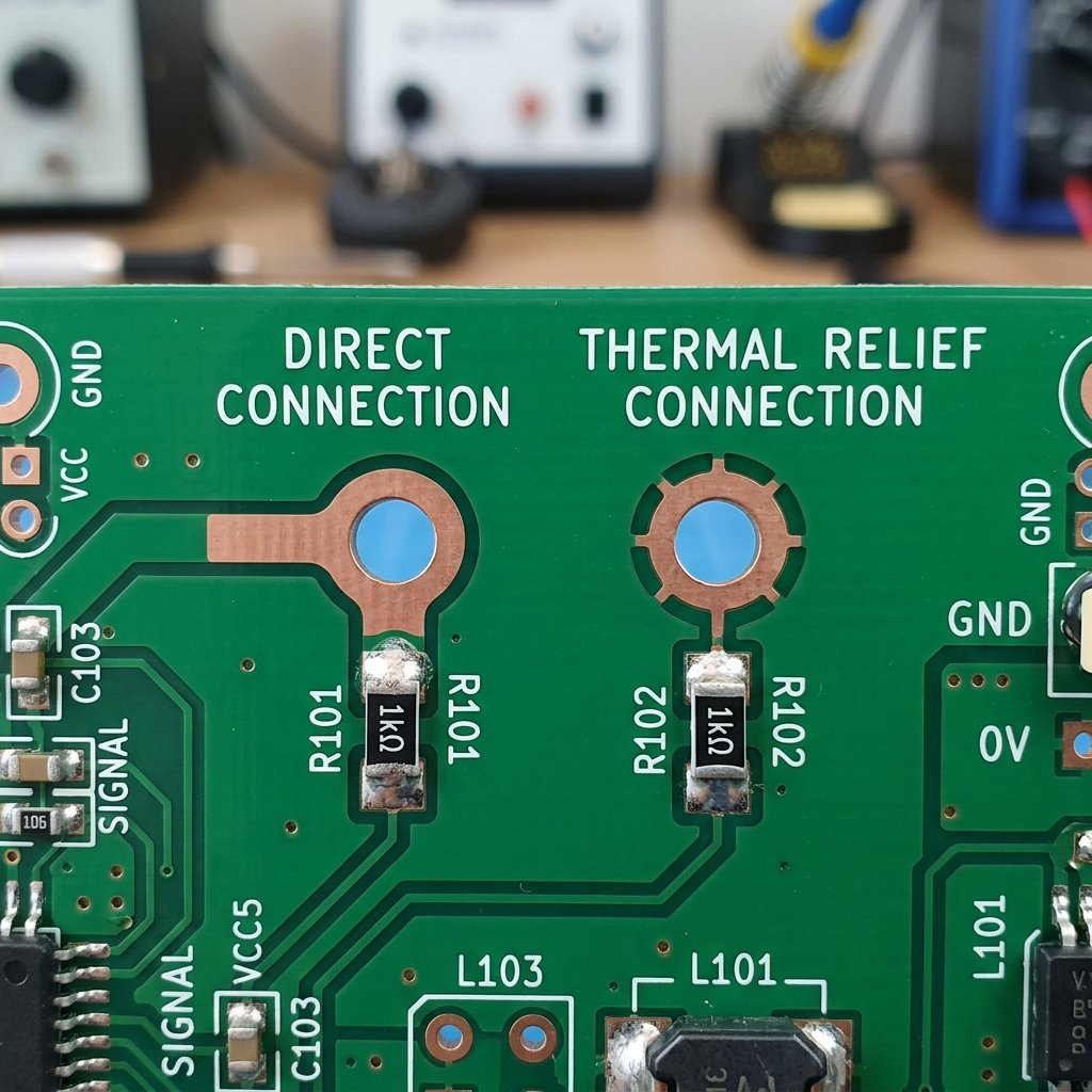
In your PCB design software’s Design Rule Check (DRC) or constraints manager, set up the default rules for thermal relief. Specify the number of spokes (usually 2 to 4), the spoke width, and the isolation gap (the space between the pad and the surrounding solid copper).
Step 3: Adjust Spoke Widths for Current Requirements
While thin spokes are great for thermal isolation, they reduce the cross-sectional area available for electrical current. For high-current pads, you must calculate the required spoke width to ensure they can carry the necessary current without overheating and acting as a fuse. Adjust the local settings for these specific pads accordingly.
Step 4: Review and Verify Connections
Once the polygon pours (copper pours) have been updated, visually inspect the thermal relief connections. Ensure that the spokes are properly formed and that no “islands” or incomplete connections have been generated, particularly in dense areas of the board.
Best Practices and Considerations
When applying thermal relief, the general rule of thumb is to use four spokes for circular pads and either two or four spokes for rectangular or square pads. The width of these spokes is a balancing act between thermal resistance (to aid soldering) and electrical conductivity (to handle the circuit’s current). For low-power digital or analog signals, standard spoke widths are usually perfectly fine. However, in power electronics, you may need to use custom shapes, wider spokes, or even solid connections (if specialized high-heat soldering equipment is available) to prioritize current-carrying capacity over ease of soldering.
Another consideration is high-frequency RF design. In RF circuits, the inductance introduced by the spokes of a thermal relief pad can negatively impact signal integrity. In such specific scenarios, RF engineers often opt for solid connections to the ground plane and manage the soldering challenges through specialized manufacturing processes, such as pre-heating the entire PCB assembly before soldering.
Frequently Asked Questions
What happens if I don’t use a thermal relief pad?
Without a thermal relief pad, the large copper plane acts as a heatsink, rapidly drawing heat away from the soldering iron. This often results in a “cold” solder joint, which has poor electrical connectivity and weak mechanical strength. It also forces the operator to apply heat for a longer time, increasing the risk of damaging the PCB or the component.
Are there situations where thermal relief should be avoided?
Yes. Thermal relief should generally be avoided in high-current power paths where the spokes might restrict current flow and cause localized heating. They are also often avoided in high-frequency RF circuits, where the spokes can introduce unwanted inductance and affect the circuit’s impedance and signal integrity.
How many spokes should a thermal relief have?
Typically, a thermal relief pad uses 2 to 4 spokes. Four spokes are standard for round and most square through-hole pads. Two spokes might be used for smaller surface mount pads or in dense routing areas where four spokes cannot be physically accommodated while maintaining design rules.