In the competitive landscape of electronics manufacturing, grasping the nuances of PCB DFM vs DFA is essential for successful product development. Design for Manufacturing (DFM) and Design for Assembly (DFA) are two critical pillars that ensure your printed circuit board (PCB) transitions smoothly from a digital concept to a physical, functional product. While they are often discussed together, they address different stages of the production process.
What is PCB DFM?
Design for Manufacturing (DFM) focuses heavily on the fabrication phase of the bare circuit board. The primary goal of DFM is to design a board that is easy and cost-effective to manufacture without sacrificing quality. This involves optimizing the physical layout, material selection, and structural characteristics to align with the capabilities of the fabrication facility.
For instance, understanding How to Determine PCB Trace Spacing to Avoid Electrical Shorts is a fundamental aspect of DFM. Adequate trace spacing prevents unintended bridging during the etching process. Similarly, paying attention to Selecting the Right PCB Hole Size for Through Hole Components ensures that the drills used during fabrication won’t break and that the plating process covers the vias and through-holes uniformly.

What is PCB DFA?
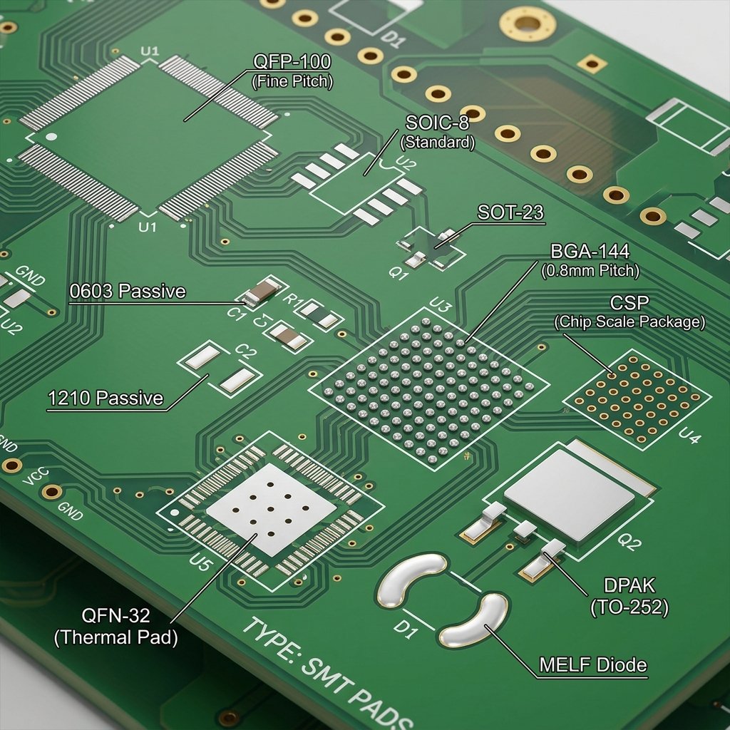
On the other hand, Design for Assembly (DFA) concerns the processes that occur after the bare board is manufactured. DFA aims to streamline the population of the board with electronic components. It considers factors like component orientation, spacing between parts to allow for automated pick-and-place machines, and thermal profiling for the soldering process.
A classic DFA consideration involves pad design and solder masks. For reliable automated assembly, following Essential PCB Pad Design Tips for Reliable SMT Assembly is crucial to prevent issues like tombstoning or skewed components. Furthermore, understanding Why PCB Solder Mask Clearance Matters for Defect-Free Soldering ensures that solder stays where it’s supposed to, reducing the risk of solder bridges between adjacent pads during the reflow process.
Comparing PCB DFM vs DFA
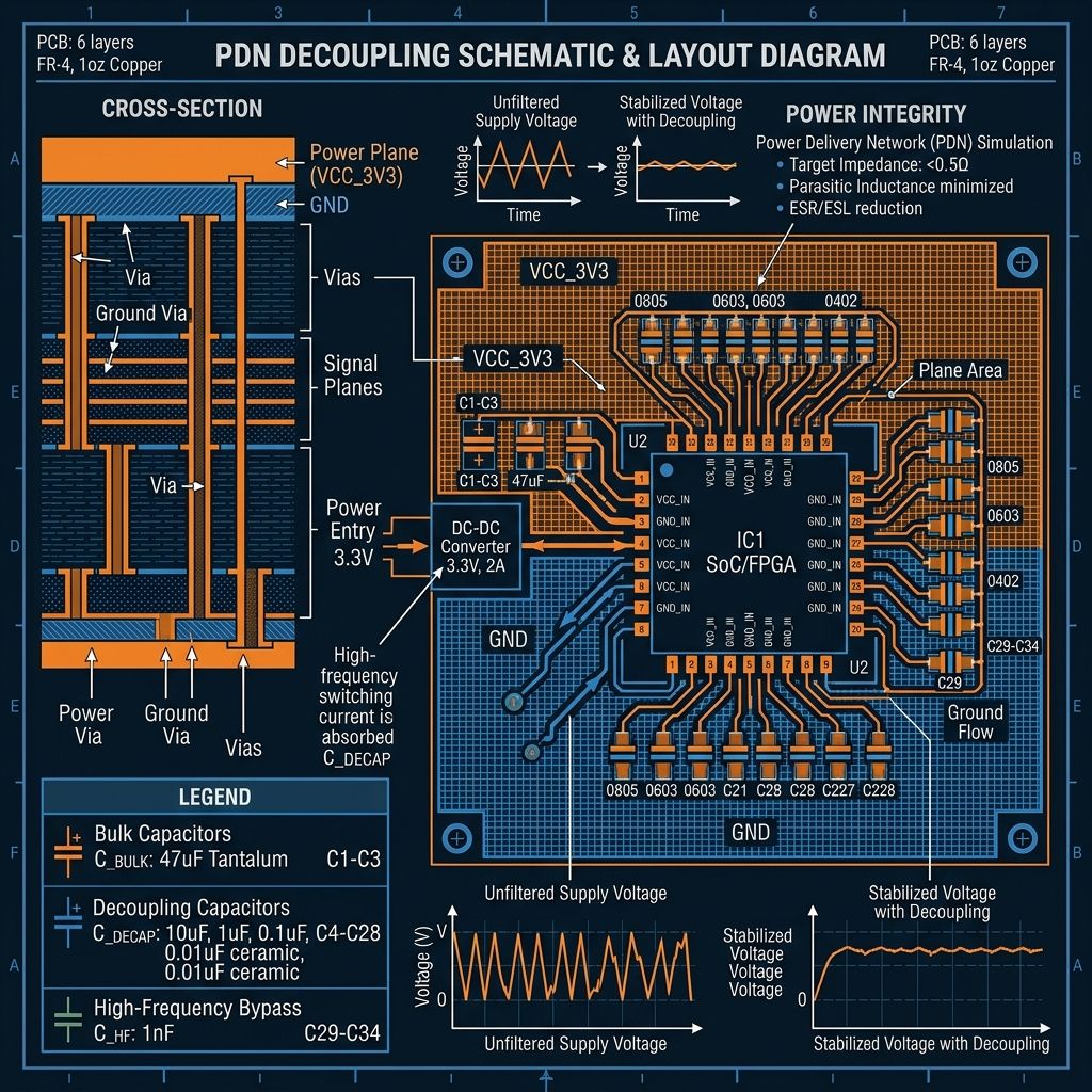
When analyzing PCB DFM vs DFA, it is helpful to view them as complementary disciplines. DFM ensures you can build the board; DFA ensures you can build the circuit. DFM looks at layers, copper weight, vias, and traces. DFA looks at the bill of materials (BOM), component footprints, clearance for soldering irons or automated placement heads, and testability. Both are vital for reducing the overall time-to-market and keeping manufacturing costs under control. Furthermore, neglecting either can lead to severe consequences. For example, poor DFM can lead to low yield rates from the fabrication plant, where many boards are discarded due to shorts or opens. Poor DFA can result in high rework rates on the assembly line, where technicians must manually fix improperly soldered components. This not only drives up costs but also introduces potential reliability issues in the field. Therefore, a holistic approach that balances both DFM and DFA is the hallmark of professional electronics design. Engineers must constantly weigh trade-offs. A design choice that makes the bare board easier to fabricate might inadvertently make component placement more difficult. The synergy between DFM and DFA ensures that the final product is not only functional but also commercially viable.
How to Implement DFM and DFA in Your Workflow
Step-by-Step Guide to Integrating DFM and DFA
1. Early Integration
2. Communication with Manufacturers
3. Component Selection
4. Prototype and Review
Frequently Asked Questions
Which is more important, DFM or DFA?
Does DFM/DFA increase design time?
Can I rely solely on my software’s DRC for DFM?
Conclusion
Mastering the concepts of PCB DFM vs DFA is indispensable for any hardware engineer or product developer. By giving equal weight to the manufacturability of the bare board and the feasibility of its assembly, you lay the groundwork for a robust, cost-efficient, and scalable electronic product. Always keep these principles in mind to navigate the complexities of product development seamlessly.