Designing a Printed Circuit Board (PCB) is a highly complex and rewarding process, demanding a blend of electrical engineering knowledge and spatial reasoning. However, no matter how perfectly your circuit simulates in software, failing to verify your design against a comprehensive PCB DFM checklist can lead to costly manufacturing delays, wasted prototypes, and functional errors. Design for Manufacturability (DFM) is the critical practice of ensuring that your digital design can actually be fabricated and assembled smoothly by the physical manufacturer.
Before you confidently click “export” to generate your Gerber files, NC Drill files, and Bill of Materials (BOM), it is imperative to pause and review your layout. By rigorously following this step-by-step PCB DFM checklist, you can proactively catch the most common and expensive mistakes that plague electronic designers.
Why You Need a PCB DFM Checklist
Every PCB fabrication house and assembly facility has strict tolerances and specific capabilities based on their equipment. If your board violates these constraints—for instance, by utilizing traces that are too thin to etch reliably, or drill holes that are too small for their mechanical bits—your design will be placed on an immediate production hold. This hold is known as an engineering query (EQ) or DFM hold, which drastically delays your production schedule and can increase costs.
A proper PCB DFM checklist acts as a vital bridge between digital theory and physical reality. It methodically guarantees that traces are robust enough to carry current without overheating, components fit correctly on their designated footprints without colliding, and everything can be assembled using automated pick-and-place machines without inducing shorts or opens. Simply put, investing time in DFM review saves money and time.
Step-by-Step PCB DFM Checklist
Follow these essential and detailed steps before releasing your PCB manufacturing files to ensure your board is fully optimized and ready for flawless production.
1. Verify Component Clearances and Footprints
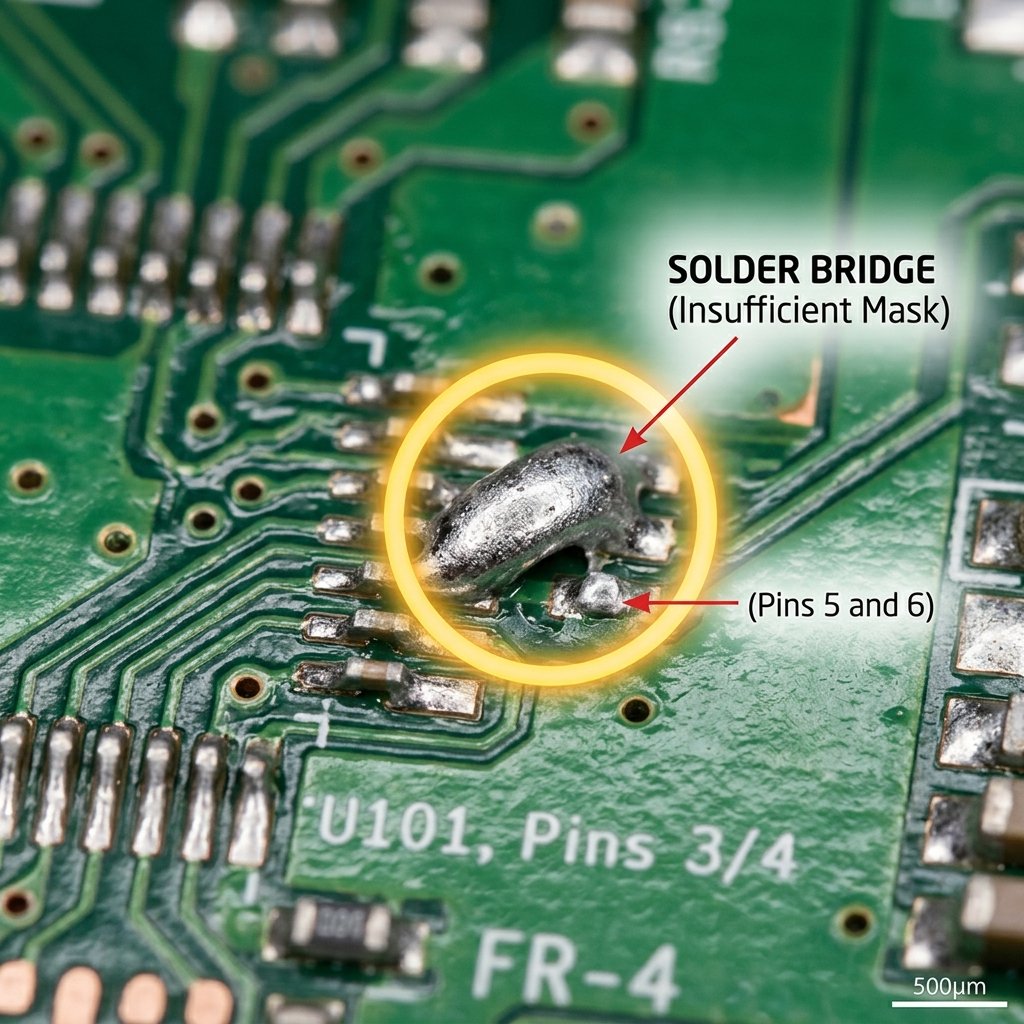
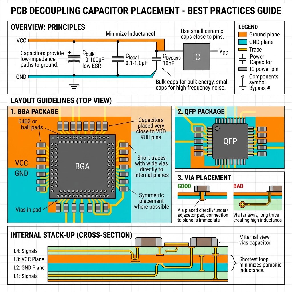
One of the single most common reasons for assembly failure is the use of incorrect component footprints. Always double-check your 3D models and component datasheets to ensure that the physical dimensions precisely match your CAD software library. Pay exceptionally close attention to the pad layout and pitch. Applying Essential PCB Pad Design Tips for Reliable SMT Assembly will save you from catastrophic manufacturing issues like solder bridging between fine-pitch ICs and the tombstoning of passive components.
2. Check Trace Width and Spacing
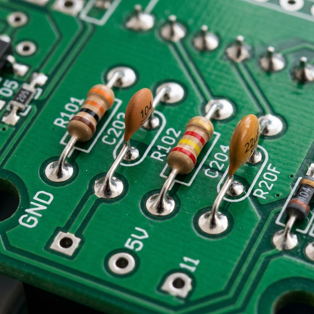
All PCB manufacturers define their absolute minimum trace widths and trace spacing capabilities. Your CAD software’s DRC (Design Rule Check) should be configured exactly with your chosen manufacturer’s capabilities before you even begin routing. Furthermore, you must guarantee that there is sufficient dielectric distance between conductive elements to prevent electrical arcing, especially in higher voltage applications. Understanding How to Determine PCB Trace Spacing to Avoid Electrical Shorts is a critical skill for designing high-density and reliable boards.
3. Review Drill Sizes and Annular Rings
It is vital to ensure that all vias and through-holes fall within the fabrication house’s standard drill chart constraints. Excessively tiny drills break easily during the manufacturing process, which directly increases your board costs. Additionally, you must calculate the annular ring size (the copper pad area surrounding the drilled hole) to prevent drill breakout during fabrication. If your electronic design heavily features through-hole parts, Selecting the Right PCB Hole Size for Through Hole Components is a fundamental and non-negotiable part of your PCB DFM checklist.
4. Optimize Copper Pour and Thermal Relief
While large solid copper polygons are excellent for shielding and current carrying, they can cause severe unequal heating during the reflow soldering process, leading to the tombstoning of small components. You should always use thermal relief pads when connecting components to massive copper planes. You can also significantly improve the board’s overall heat management and reliability by studying How to Optimize PCB Copper Pour for Better Thermal Dissipation.
5. Validate Silkscreen and Solder Mask
Silkscreen ink that accidentally overlaps onto exposed copper pads will inevitably cause major solderability issues, resulting in weak or failed mechanical joints. You must verify that all reference designators, logos, and polarity markings are legible, properly oriented, and completely clipped away from all exposed pads. Furthermore, solder mask openings (the mask expansion) must be sufficiently large to comfortably accommodate manufacturing registration tolerances, preventing the solder mask from inadvertently covering pads.
The Importance of Communication with Your Fab House
Ultimately, your PCB DFM checklist is only as effective as the technical data you receive from your chosen manufacturer. It is a best practice to always request their detailed capabilities document before starting a design. Input those exact minimum and maximum values directly into your CAD software’s DRC engine. Doing this proactively prevents the dreaded DFM hold and ensures your printed circuit boards are fabricated exactly as you envisioned them.
Frequently Asked Questions About PCB DFM
What exactly is a PCB DFM checklist?
A PCB DFM checklist is a comprehensive, structured set of design rules, verifications, and best practices that ensure a printed circuit board layout can be reliably and cost-effectively manufactured in a real-world facility. It thoroughly covers aspects like trace spacing, pad sizes, drill hole tolerances, component clearances, and solder mask expansion.
Why is trace spacing such a critical part of DFM?
Trace spacing is incredibly critical because if copper traces are placed too close to one another, they can accidentally short out during the chemical etching process at the factory. In high-voltage designs, insufficient spacing can also cause dangerous electrical arcing. Rigorously checking trace spacing is a mandatory, non-skippable step in any professional DFM process.
How does component placement affect board manufacturability?
Placing electronic components too close to the physical edge of the board, or placing them too close to each other, can cause severe issues with automated pick-and-place machinery, wave soldering, and automated optical inspection (AOI). A good DFM check ensures there is always enough physical clearance for robotic assembly and testing probes.