현대 전자 산업에서 소형화는 가장 중요한 요소입니다. 소비자들의 기대가 더 작고, 더 가볍고, 더 뛰어난 성능을 갖춘 전자제품으로 옮겨감에 따라, 고효율 인쇄회로기판(PCB) 레이아웃에 대한 필요성도 기하급수적으로 증가했습니다. 이러한 공간 효율성에 대한 끊임없는 추구가 바로 고밀도 상호연결(HDI) 기판과 블라인드 비아 기술이 주목받는 이유입니다. 블라인드 비아는 기판을 완전히 관통하지 않고 보드의 외부 층과 내부 층을 전략적으로 연결함으로써 중요한 배선 공간을 확보해 줍니다. 이를 통해 전기 엔지니어들은 매우 제한된 설치 공간에 훨씬 더 많은 기능, 부품 및 트레이스를 집적할 수 있습니다. 정확히 이해하면 스마트 기기가 콤팩트한 설계를 위해 HDI PCB 적층 구조가 필요한 이유 이는 블라인드 비아 기술이 발휘할 수 있는 레이아웃의 잠재력을 온전히 이해하기 위한 기초 단계입니다.
블라인드 비아 기술이란 무엇인가요?
A blind via is a specialized type of interconnection used in multi-layer printed circuit boards. It connects the top or bottom outer layer of the PCB to one or more immediately adjacent inner layers but deliberately stops short of penetrating the entire thickness of the board. Because it is only visible and accessible from one side of the board—referred to as the “blind” side—it leaves the opposite exterior surface completely intact and untouched. This pristine area on the opposite side can subsequently be used for placing additional surface mount technology (SMT) components, or it can be utilized for routing more complex traces, dramatically increasing the board’s overall component and routing density.
이와는 극명한 대조를 이루는 표준 스루홀 비아는 회로 기판 전체를 위에서 아래로 관통합니다. 제조는 더 간단하지만, 스루홀 비아는 전기적 연결이 실제로 필요하지 않은 층을 포함해 모든 내부 및 외부 층에서 귀중한 기판 면적을 과도하게 차지합니다. 블라인드 비아 기술을 적용하는 것은 특히 공간이 제한된 첨단 설계를 다룰 때 매우 중요합니다. 예를 들어, 10층 PCB 스택업을 통해 복잡한 전원 요구 사항 관리, 견고하고 끊김 없는 전원 및 접지 평면의 구조적·전기적 무결성을 유지하기 위해서는 스루홀 비아의 사용을 최소화하는 것이 절대적으로 필수적입니다.
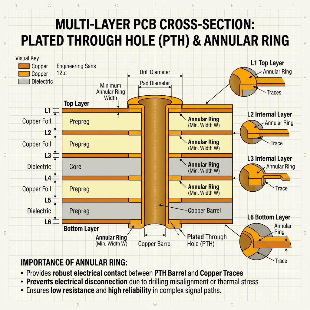
PCB 설계에서 블라인드 비아를 구현하는 방법
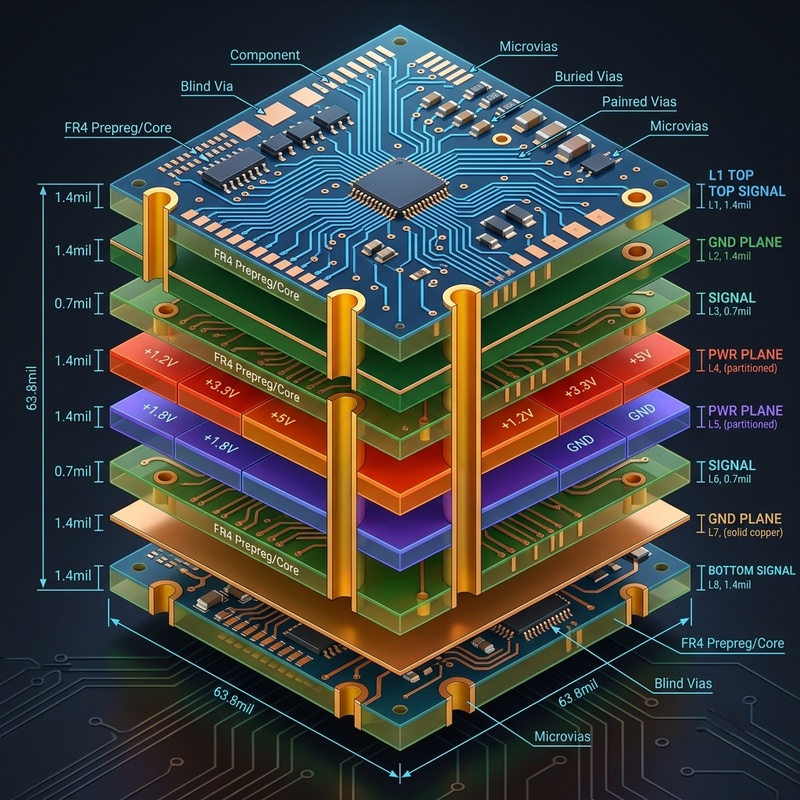
블라인드 비아를 활용한 설계 전략
이러한 체계적인 단계를 따름으로써 블라인드 비아 기술을 활용한 신뢰성 높고 제조성이 뛰어난 HDI PCB 설계를 보장할 수 있습니다.
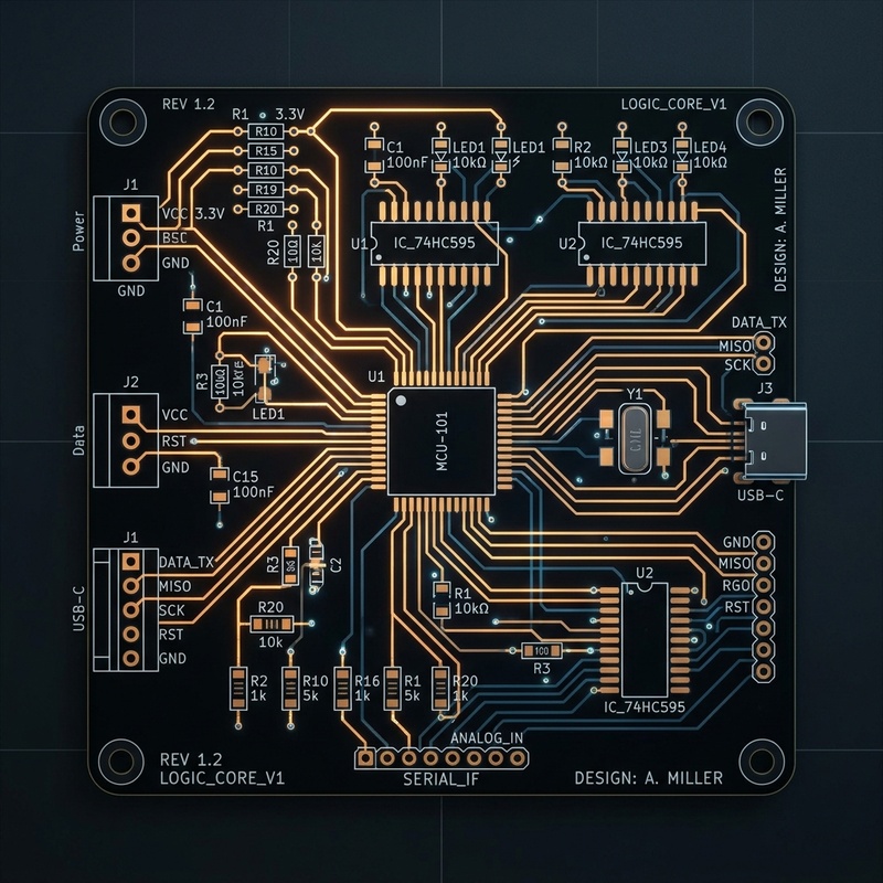
블라인드 비아 기술이 가져다주는 혁신적인 이점
The primary and most immediately apparent advantage of employing blind via technology is the massive, transformative increase in available board real estate. By completely freeing up segments of different layers, designers are empowered to achieve significantly shorter signal paths. These shorter paths inherently improve signal integrity and simultaneously reduce harmful electromagnetic interference (EMI). Furthermore, utilizing fewer through-hole vias mathematically translates to fewer impedance discontinuities along critical signal paths, which is an absolutely vital consideration for modern high-speed digital designs. While blind vias do undeniably add complexity and a premium cost to the bare board manufacturing process—typically requiring advanced sequential lamination cycles or precision laser drilling—the spatial trade-off is almost always necessary and well worth it for producing cutting-edge smart devices, wearable tech, and sophisticated medical instrumentation.