تكنولوجيا «Via» من الجيل التالي في مجال تصميم الدوائر المطبوعة عالية الكثافة (HDI) للأجهزة الإلكترونية القابلة للارتداء
The evolution of wearable devices has pushed the boundaries of miniaturization, demanding smaller, lighter, and more powerful components. At the heart of this revolution is next generation hdi via technology. High-Density Interconnect (HDI) printed circuit boards rely on advanced via structures to route complex signals within an incredibly compact footprint. In this comprehensive guide, we’ll explore how next generation hdi via solutions are transforming the landscape of wearable electronics, overcoming traditional manufacturing limitations, and paving the way for smarter, more efficient wearable technology.
The Need for Advanced Interconnects in Wearables
Wearable technology, ranging from everyday smartwatches and fitness trackers to advanced medical monitoring patches and augmented reality glasses, requires electronic circuits that can fit seamlessly into everyday items. This size constraint leaves traditional PCB manufacturing struggling to keep up with the demands for higher functionality. As component pitches become finer and ball grid arrays (BGAs) shrink in size, the need for advanced routing techniques is paramount. By leveraging state-of-the-art HDI PCB manufacturing techniques, design engineers can achieve the necessary component density without compromising on signal integrity, thermal management, or overall device reliability. The shift toward tighter packaging makes it absolutely critical to adopt advanced interconnection methodologies.
Understanding Next Generation HDI Via Structures
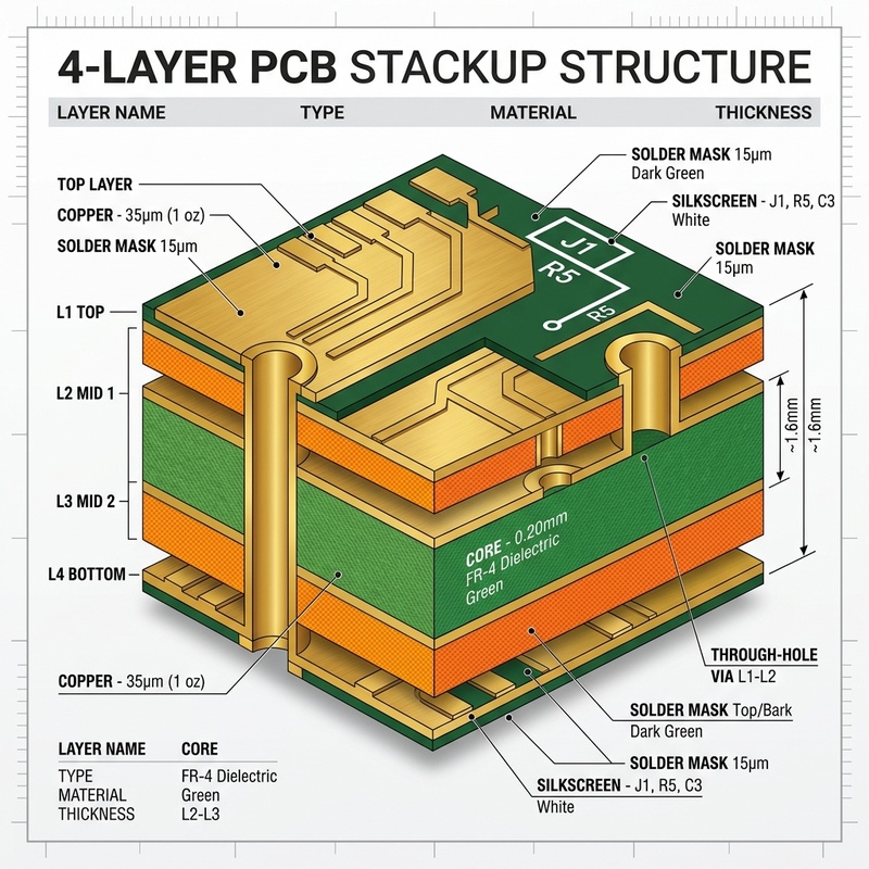
Next generation hdi via technology primarily revolves around the extensive use of microvias, stacked vias, and staggered vias. These micro-structures allow for ultra-high-density routing across multiple layers of a printed circuit board. Unlike traditional mechanical drilling, which is limited by the physical size of drill bits and mechanical tolerances, advanced microvias are typically created using precision laser drilling technology. This enables via diameters of 0.15mm (6 mils) or even less, making them ideal for the highly constrained spaces found in modern wearables.
When designers employ stacked microvias, they can connect multiple adjacent layers sequentially without consuming valuable routing space on the layers in between. By integrating advanced microvia technology in wearables, designers can significantly reduce the overall board size, improve electrical performance by shortening signal paths, and create more robust connections for high-frequency signal transmission.
Advantages for the Wearable Electronics Market
The implementation of next generation hdi via architectures brings several distinct and highly sought-after advantages to the wearable electronics market. These benefits are critical for keeping up with consumer expectations for lighter, longer-lasting, and more feature-rich devices:
- Extreme Miniaturization: Allows for significantly smaller and lighter devices that remain comfortable to wear all day long without sacrificing computational power.
- سلامة الإشارة المحسّنة: Shorter interconnect lengths heavily reduce parasitic capacitance and inductance, which is a crucial factor for maintaining the integrity of high-speed digital and RF signals in Bluetooth and Wi-Fi enabled wearables.
- موثوقية محسّنة: Advanced via filling and plating techniques ensure the structural integrity of the PCB. This is especially important for wearables that undergo constant physical stress, temperature fluctuations, and exposure to moisture.
- Design Flexibility and Form Factor Innovation: Combining high-density interconnects with rigid-flex PCB solutions allows for highly innovative form factors. Designers can create circuits that literally bend, fold, and flex with the human body, enhancing both ergonomics and durability.
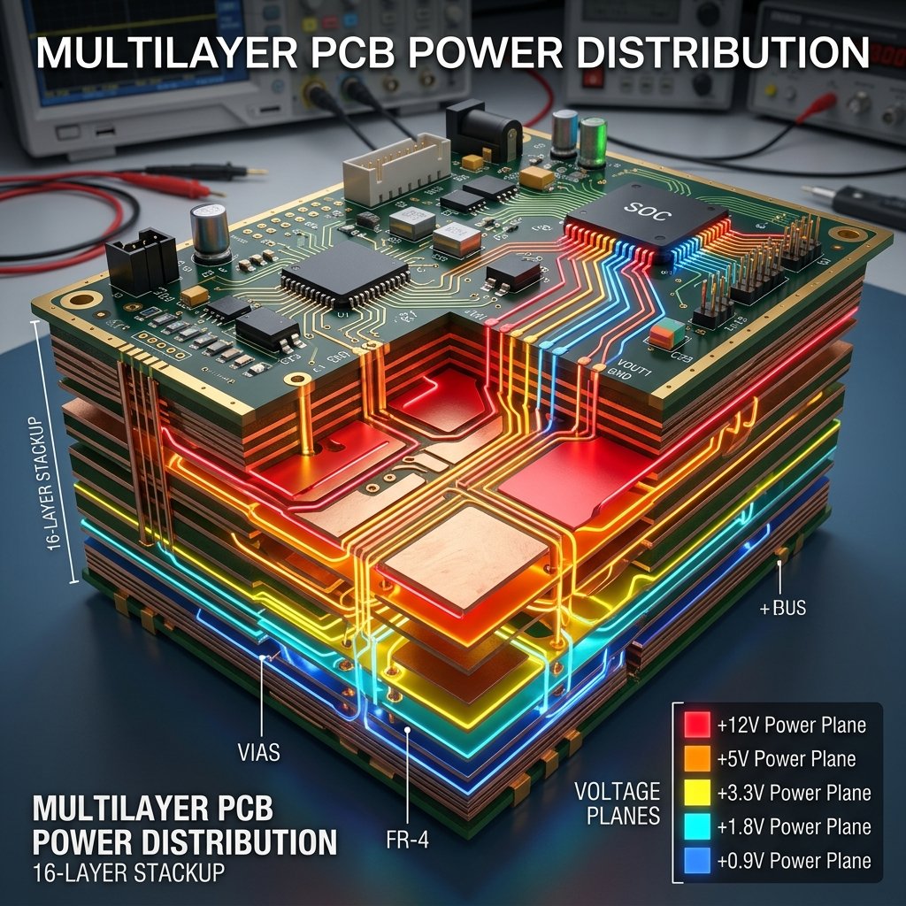
How to Design with Next Generation HDI Via for Wearables
A comprehensive brief guide on incorporating advanced HDI via structures into your next wearable device PCB design, ensuring maximum performance and manufacturability.
Step 1: Determine Layer Stackup and Select Materials
Start the design process by selecting the appropriate advanced PCB materials that specifically support fine lines, tight spaces, and sequential lamination. Define a layer stackup that intelligently utilizes blind and buried vias to free up routing space on critical signal layers.
Step 2: Implement Advanced Microvia Structures
Use staggered or stacked microvias instead of traditional through-hole vias whenever possible. By implementing via-in-pad (VIP) technology, you can route directly out from under dense BGA components, clearing routing channels on inner layers and significantly increasing the board’s routing density.
Step 3: Focus on Signal Integrity and Power Delivery
Ensure that your next generation hdi via design accounts for robust return paths and a stable power distribution network (PDN). Always place ground return vias very close to signal transitions across layers. This maintains a continuous and low-impedance return path for high-frequency signals, reducing electromagnetic interference (EMI).
Step 4: Collaborate with Your PCB Manufacturer Early On
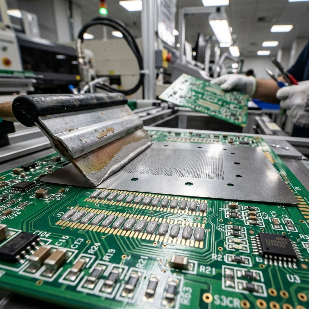
Communicate early and frequently with your chosen PCB fabrication house. It is vital to ensure that they possess the high-precision laser drilling capabilities, stringent process controls, and specialized plating techniques necessary to yield reliable, defect-free microvia structures in mass production.
الأسئلة الشائعة (FAQ)
What exactly defines a next generation hdi via?
A next generation hdi via typically refers to advanced laser-drilled microvias (usually less than 0.15mm in diameter) that are stacked or staggered across multiple sequential lamination layers. These vias allow for extreme routing density, utilizing techniques like via-in-pad plated over (VIPPO) to accommodate the complex requirements of modern miniature electronics like wearable devices.
Why is HDI technology absolutely critical for modern wearable devices?
Wearable devices require immense processing power, diverse sensor arrays, and wireless connectivity within a very limited physical space. Traditional PCBs cannot route the high pin-count components used today. HDI technology allows designers to cram more components onto a significantly smaller PCB footprint by utilizing microscopic vias and extremely fine line widths, achieving unprecedented miniaturization.
Are there specific manufacturing challenges associated with next generation hdi via?
Yes, manufacturing these advanced via structures presents several significant challenges. It requires highly precise laser drilling alignment, rigorous and void-free copper plating processes (especially for stacked microvias), and extremely strict control over material registration during multiple sequential lamination cycles. Partnering with an experienced HDI manufacturer is essential for success.
الخاتمة
As the demand for more capable, feature-rich, and incredibly compact wearable devices continues to soar globally, the role of next generation hdi via technology will only become more prominent. By mastering both the design intricacies and the manufacturing nuances of these advanced interconnect structures, engineers can overcome traditional limitations and consistently create the next wave of innovative wearable electronics that seamlessly and unobtrusively integrate into our daily lives.