عندما يتعلق الأمر بتصميم لوحات الدوائر المطبوعة (PCB)، فإن أحد الجوانب الأكثر أهمية لضمان سلامة الإشارة ويتمثل أحد أهم العوامل في الحد من التداخل الكهرومغناطيسي (EMI) في تنفيذ مستوى أرضي فعال في لوحات الدوائر المطبوعة (PCB). ففي التصميمات عالية السرعة وتصميمات الإشارات المختلطة، يمكن أن تشكل الطريقة التي تتعامل بها مع مسارات العودة الأرضية الفارق بين لوحة تجتاز اختبارات التوافق الكهرومغناطيسي (EMC) وأخرى تفشل فشلاً ذريعاً. في هذا الدليل الشامل، سنتناول المفاهيم الأساسية لأسطح التأريض، وأسباب أهميتها في تقليل الضوضاء، وأفضل الممارسات العملية التي يمكنك تطبيقها في مشروع تصميم لوحات الدوائر المطبوعة (PCB) القادم.
ما هو مستوى التأريض في لوحات الدوائر المطبوعة (PCB)؟
سطح التأريض في لوحة الدوائر المطبوعة (PCB) هو مساحة واسعة من رقائق النحاس الموجودة على لوحة الدوائر المطبوعة، وهي متصلة بطرف التأريض في مصدر الطاقة. وهو يعمل كـ... مسار الإرجاع لتوصيل التيار من العديد من المكونات المختلفة. في اللوحات متعددة الطبقات، غالبًا ما تُخصص طبقة كاملة لمستوى التأريض. وتوفر هذه المساحة الكبيرة مسارًا عائداً ذو مقاومة منخفضة جدًّا للتيارات الكهربائية، وهو أمر بالغ الأهمية للدوائر الرقمية عالية السرعة والدوائر التناظرية عالية التردد.
لماذا يُعد المستوى الأرضي مهمًا لتقليل الضوضاء؟
يمكن أن تنشأ الضوضاء في لوحة الدوائر المطبوعة (PCB) من مصادر متنوعة، بما في ذلك التداخل بين المسارات المتجاورة، وارتداد التيار الأرضي الناتج عن التبديل المتزامن للمخرجات، والتداخل الكهرومغناطيسي الخارجي (EMI). ويعالج المستوى الأرضي المستمر ذو المقاومة المنخفضة هذه المشكلات بشكل مباشر:
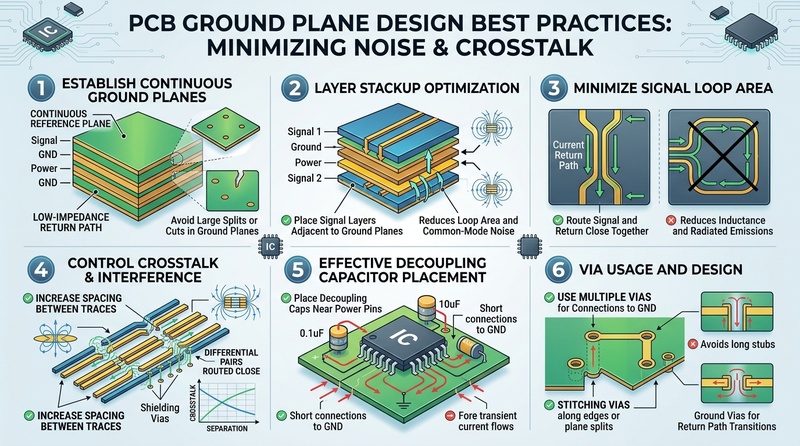
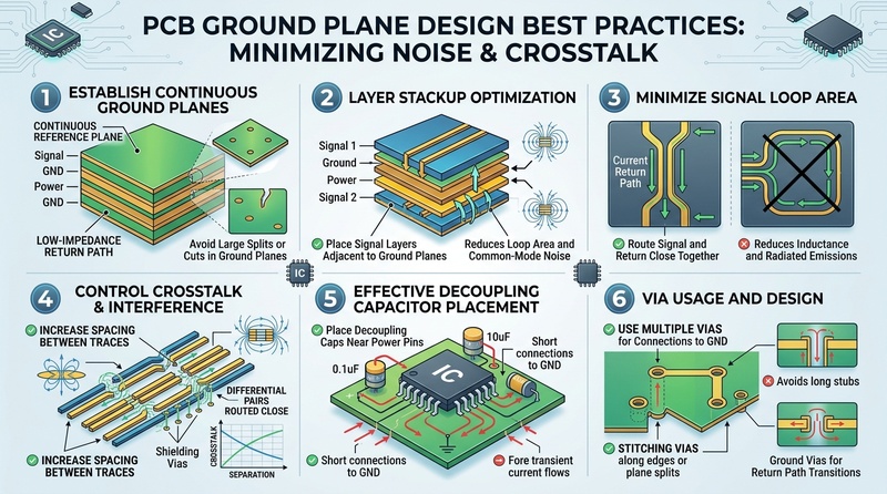
- مساحة الحلقة المخفضة: يجب أن يكون لكل إشارة مسار عودة إلى مصدرها. ومن الطبيعي أن تتبع الإشارات عالية التردد المسار الأقل مقاومة حثية، والذي يقع مباشرةً أسفل مسار الإشارة. ويضمن وجود مستوى أرضي متين أن يكون مسار العودة هذا أقرب ما يمكن من مسار الإشارة، مما يقلل مساحة الحلقة إلى أدنى حد. وتؤدي مساحة الحلقة الأصغر إلى تقليل التداخل الكهرومغناطيسي المشع (EMI) وتقليل التعرض للضوضاء الخارجية.
- مقاومة أرضية أقل: تتميز مسارات النحاس بمقاومة وحث داخليين. وعندما تتشارك عدة مكونات في مسار أرضي ضيق، يمكن أن تتسبب التيارات العائدة في حدوث انخفاضات في الجهد (V = I * Z)، مما يؤدي إلى حدوث «ارتداد الأرض» وتدهور هوامش الضوضاء. وتتميز الصفيحة النحاسية السميكة بمقاومة أقل بكثير، مما يقلل من هذه الفروق في الجهد إلى أدنى حد.
- التدريع: يمكن أن يعمل المستوى الأرضي الصلب كدرع كهرومغناطيسي، حيث يحمي طبقات الإشارات الداخلية الحساسة من مصادر الضوضاء الخارجية ويمنع الإشارات الداخلية عالية التردد من الانتشار إلى الخارج.
كيفية تصميم مستوى أرضي فعال
اتبع هذه الخطوات لتحسين مستوى أرضية لوحة الدوائر المطبوعة (PCB) بهدف تقليل التشويش إلى أدنى حد ممكن وضمان أقصى قدر من سلامة الإشارة.
الخطوة 1: استخدام طبقات أرضية مخصصة
في لوحات الدوائر المطبوعة متعددة الطبقات (4 طبقات أو أكثر)، احرص دائمًا على تخصيص طبقة كاملة واحدة على الأقل لمستوى التأريض. ضع طبقات الإشارات الحساسة عالية السرعة مباشرةً بجوار مستوى التأريض الصلب هذا لتقليل محاثة مسار العودة إلى أدنى حد ممكن.
الخطوة 2: تجنب تقسيم مستوى التأريض
من أفضل الممارسات عمومًا الحفاظ على استمرارية مستوى التأريض. فقد يؤدي تقسيم مستوى التأريض إلى أقسام منفصلة للتناظرية والرقمية إلى ظهور فجوات تجبر تيارات العودة على السير في مسارات أطول وأكثر حثية حول الفجوة، مما يؤدي إلى زيادة كبيرة في التداخل الكهرومغناطيسي (EMI). وإذا كان لا بد من تقسيم المستوى، فتأكد من عدم عبور أي مسارات إشارة عبر نقطة التقسيم.
الخطوة 3: إدارة مسارات الإرجاع ذات الإشارات المختلطة بعناية
بالنسبة للوحات التي تحتوي على دوائر تناظرية ورقمية على حد سواء، استخدم مستوى أرضي واحد متواصل، ولكن قم بتقسيم المكونات ومسارات التوصيل. احرص على إبقاء المكونات والمسارات التناظرية في منطقة واحدة، والمكونات والمسارات الرقمية في منطقة أخرى، مع التأكد من أن تيارات العودة الخاصة بها لا تتداخل مع المجال الآخر.
الخطوة 4: استخدم ثقوب التوصيل الأرضية بكثرة
عندما تنتقل الإشارة من طبقة إلى أخرى، يجب أن يجد تيار العودة الخاص بها أيضًا مسارًا إلى المستوى المرجعي الجديد. ضع ثقب توصيل أرضي (ثقب ربط) بجوار ثقب الإشارة مباشرةً. بالإضافة إلى ذلك، استخدم ثقوب الربط حول محيط اللوحة لربط مستويات الأرضية المتعددة معًا ومنع تأثيرات الإشعاع من الحواف.
الأسئلة الشائعة (FAQ)
هل يجب أن أستخدم طريقة «صب المضلع» أم طبقة مخصصة لسطح الأرض؟
بالنسبة للوحات ذات الطبقتين، فإن الطريقة المعتادة تتمثل في صب مساحة متعددة الأضلاع على كل من الطبقتين العلوية والسفلية، تربط بينهما العديد من الثقوب الموصلة. ومع ذلك، بالنسبة للوحات ذات 4 طبقات أو أكثر، يُوصى بشدة باستخدام طبقة داخلية مخصصة لمستوى التأريض، حيث إنها توفر خصائص مقاومة منخفضة فائقة وحماية أفضل.
ماذا يحدث إذا عبر مسار إشارة أحد الانقسامات في مستوى التوصيل الأرضي؟
إذا عبر مسار إشارة عالية السرعة شقًا أو فجوة في مستوى التأريض الأساسي، فلن يتمكن التيار العائد من التدفق مباشرةً أسفل المسار. بل سيتعين عليه إيجاد مسار أطول حول الشق، مما يؤدي إلى زيادة مساحة الحلقة، وزيادة الحث، وتدهور سلامة الإشارة، وخلق مصدر كبير للإشعاع الكهرومغناطيسي (EMI). تجنب دائمًا توجيه المسارات فوق شق في مستوى التأريض.
كيف تؤثر المسافة بين طبقة الإشارة ومستوى التأريض على الضوضاء؟
كلما اقترب مسار الإشارة من مستوى الأرض المرجعي، زادت قوة الاقتران بينهما. ويؤدي هذا الاقتران الأقوى إلى تقليل مساحة الحلقة والمحاثة الطفيلية لمسار العودة، مما يؤدي مباشرةً إلى انخفاض التداخل الكهرومغناطيسي (EMI) وتقليل التداخل بين الإشارات وتحسين سلامة الإشارة بشكل عام. ولهذا السبب غالبًا ما تُفضل العوازل الرقيقة في التراكيب عالية السرعة.
الخاتمة
إن تصميم مستوى أرضي قوي للوحة الدوائر المطبوعة (PCB) ليس أمراً ثانوياً؛ بل هو عنصر أساسي في أي تصميم إلكتروني ناجح. ومن خلال فهم كيفية تدفق تيارات العودة وإعطاء الأولوية لمسار متواصل ومنخفض المقاومة، يمكنك تقليل الضوضاء بشكل كبير، ومنع الأعطال الناتجة عن التداخل الكهرومغناطيسي (EMI)، وضمان تشغيل دوائرك بشكل موثوق عبر جميع الترددات المقصودة.