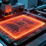
في عالم الإلكترونيات الذي يشهد تطوراً سريعاً، يُعد تصميم لوحة الدوائر المطبوعة (PCB) القادرة على معالجة الإشارات عالية السرعة دون المساس بالأداء أمراً بالغ الأهمية. وغالبًا ما يمثل التصميم الجيد للوحة الدوائر المطبوعة المكونة من 6 طبقات الحل الأمثل للعديد من المهندسين الذين يحتاجون إلى طبقات توجيه أكثر مما توفره اللوحة المكونة من 4 طبقات، إلى جانب حماية أفضل من التداخل الكهرومغناطيسي (EMI) وسلامة الإشارة. في هذا الدليل الشامل، سنتعمق في آليات تحسين تصميم لوحة الدوائر المطبوعة المكونة من 6 طبقات لضمان سلامة إشارات قوية، وتداخل منخفض، وتوصيل ممتاز للطاقة.
فهم تركيب لوحات الدوائر المطبوعة المكونة من 6 طبقات
تتكون لوحة الدوائر المطبوعة (PCB) القياسية ذات الست طبقات من ست طبقات من النحاس الموصّل، تفصل بينها مواد عازلة كهربائياً مثل FR-4. وتلعب طريقة ترتيب هذه الطبقات — أي «ترتيب الطبقات» — دوراً أساسياً في كيفية انتشار الإشارات الكهربائية عبر اللوحة. وإذا قمت بتخصيص طبقات الإشارة والطاقة والتأريض بشكل عشوائي، فإنك تخاطر بحدوث مشاكل خطيرة تتعلق بسلامة الإشارة. ويبدو التراص النموذجي عالي الفعالية المكون من 6 طبقات لضمان سلامة الإشارة كما يلي:
- الطبقة 1: الإشارة العليا
- الطبقة 2: مستوى التأريض (GND)
- الطبقة 3: الإشارة الداخلية 1
- الطبقة الرابعة: مستوى الطاقة (PWR)
- الطبقة 5: مستوى التأريض (GND)
- الطبقة 6: الإشارة السفلية
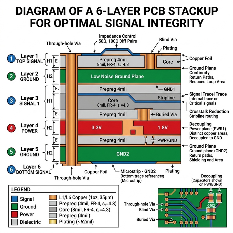
يضمن هذا الترتيب المحدد أن تكون جميع طبقات الإشارات مجاورة لمستوى مرجعي صلب واحد على الأقل. دعونا نستكشف سبب أهمية ذلك البالغة في تحسين تصاميمكم عالية السرعة.
دور المستويات المرجعية في سلامة الإشارة
عندما تنتقل إشارة على طول مسار، يجب أن يجد تيار العودة طريقه للعودة إلى المصدر. وبطبيعة الحال، فإن تيارات العودة عالية التردد تبحث عن المسار الأقل حثًا، والذي يقع مباشرةً أسفل مسار الإشارة على المستوى المرجعي المجاور. ومن خلال توفير مستويات أرضية أو مستويات طاقة متصلة وغير منقطعة بجوار طبقات الإشارة مباشرةً، يمكنك تقليل مساحة حلقة الدائرة إلى أدنى حد. وتؤدي مساحة الحلقة الأصغر مباشرةً إلى انخفاض الحث الطفيلي، وتقليل انبعاثات التداخل الكهرومغناطيسي (EMI)، وتحسين سلامة الإشارة.
تقليل التداخل بين الطبقات إلى أدنى حد
في اللوحة المكونة من 6 طبقات، يتوفر لديك مساحة أكبر لتوجيه المسارات، ولكنك تتعرض أيضًا لخطر التداخل بين طبقات الإشارات المتجاورة إذا لم تتوخى الحذر. على سبيل المثال، إذا كانت الطبقة 3 والطبقة 4 كلاهما طبقات إشارات دون وجود مستوى مرجعي بينهما، فقد تتداخل الإشارات بسهولة مع بعضها البعض. للتخفيف من هذا الأمر، قم دائمًا بتوجيه طبقات الإشارات المتجاورة بشكل متعامد (عمودي) مع بعضها البعض إذا لم تكن مفصولة بمستوى مرجعي. ومع ذلك، في التراص المُحسّن لدينا (Top-GND-Sig1-PWR-GND-Bot)، تحتوي كل طبقة إشارة على مستوى مرجعي مخصص، مما يقلل بشكل كبير من التداخل الجانبي.
التحكم في المعاوقة والمسافة العازلة
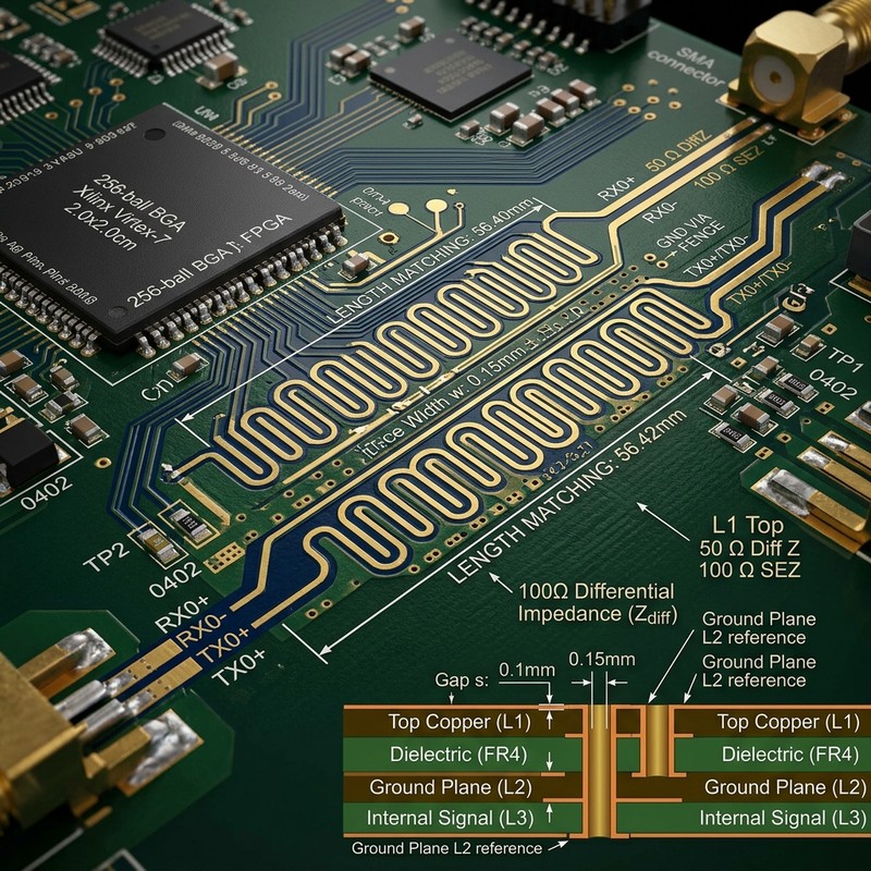
تتطلب الواجهات عالية السرعة مثل USB وHDMI وPCIe الالتزام الصارم بـ المقاومة المُحكومة لمنع انعكاسات الإشارات. في تركيبة مكونة من 6 طبقات، يمكنك تحقيق ذلك من خلال الاختيار الدقيق لسمك المواد العازلة (المواد المُسبقة التشريب واللب) بين مسارات الإشارات ومستويات الإشارة المرجعية الخاصة بها. عن طريق ضبط عرض التتبع وبفضل التباعد العازل، يمكنك ضبط مقاومات دقيقة أحادية الطرف (مثل 50 أوم) وتفاضلية (مثل 90 أو 100 أوم). يُنصح بشدة بالتعاون عن كثب مع الشركة المصنعة للوحات الدوائر المطبوعة (PCB) للحصول على ملف مقاومة دقيق لتكوين لوحات الدوائر المطبوعة ذات الست طبقات الخاصة بك قبل البدء في عملية التوجيه.
كيفية تصميم تركيب مثالي للوحة الدوائر المطبوعة المكونة من 6 طبقات
اتبع هذه الإرشادات التفصيلية خطوة بخطوة لتصميم تراكب لوحات الدوائر المطبوعة (PCB) المكون من 6 طبقات، مع التركيز على تعظيم سلامة الإشارة وتقليل التداخل الكهرومغناطيسي (EMI) إلى أدنى حد.
الخطوة 1: تحديد تخصيصات الطبقات
الخطوة 2: حساب متطلبات المعاوقة
الخطوة 3: تخطيط مستويات الطاقة والتأريض
الخطوة 4: توجيه الإشارات الحيوية أولاً
اعتبارات تتعلق بسلامة الإمداد بالطاقة
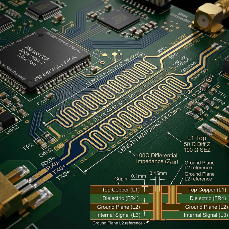
ترتبط سلامة الإشارة وسلامة الطاقة ارتباطًا وثيقًا. فقد يتداخل مصدر الطاقة الذي يعاني من التشويش مع إشاراتك عالية السرعة، مما يتسبب في حدوث تذبذب أو أخطاء في البيانات. وفي اللوحة المكونة من 6 طبقات، يؤدي وضع مستويي الطاقة والأرضية بالقرب من بعضهما (مثل الطبقتين 4 و5 في مثالنا) إلى تكوين سعة كهربائية بين المستويين. تساعد هذه السعة المدمجة على قمع الضوضاء عالية التردد في شبكة توزيع الطاقة (PDN)، مما يضمن وصول طاقة نظيفة إلى المكونات. بالإضافة إلى ذلك، فإن وضع مكثفات الفصل بالقرب من دبابيس الطاقة للأجهزة النشطة سيساهم في زيادة استقرار الجهد وتحسين الأداء العام للنظام.
الأسئلة الشائعة (FAQ)
ما هو أفضل ترتيب لطبقات لوحات الدوائر المطبوعة (PCB) المكونة من 6 طبقات؟
أفضل تكوين لطبقات لوحات الدوائر المطبوعة (PCB) المكونة من 6 طبقات للتصميمات العامة عالية السرعة هو: الطبقة العلوية للإشارات،, المستوى الأرضي, ، إشارة داخلية، مستوى الطاقة، مستوى التأريض، إشارة سفلية. ويوفر ذلك مستويات مرجعية ممتازة وحماية من التداخل الكهرومغناطيسي.
لماذا يُفضل استخدام لوحة دوائر مطبوعة ذات 6 طبقات بدلاً من لوحة ذات 4 طبقات؟
تتيح لوحة الدوائر المطبوعة (PCB) المكونة من 6 طبقات إضافة طبقتين إضافيتين للإشارات مع الحفاظ على مستويات أرضية وطاقة متينة. ويؤدي ذلك إلى زيادة كثافة التوجيه، كما يتيح تحسين سلامة الإشارة والتحكم في المعاوقة في اللوحات المعقدة.
هل يمكنني استخدام عدة مستويات طاقة في تركيبة مكونة من 6 طبقات؟
نعم، يمكنك تقسيم طبقة الطاقة (مثل الطبقة 4) إلى عدة مسارات نحاسية لدعم مجالات جهد كهربائي مختلفة (مثل 3.3 فولت، 1.8 فولت، إلخ). ومع ذلك، تجنب توجيه الإشارات الحرجة عالية السرعة عبر نقاط التقسيم في طبقة الطاقة، لأن ذلك يقطع الاستمرارية مسار الإرجاع.
الخاتمة
يُعد إتقان تصميم طبقات لوحات الدوائر المطبوعة (PCB) المكونة من 6 طبقات مهارة أساسية في تصميم الإلكترونيات الحديثة. ومن خلال إعطاء الأولوية لمسارات العودة المستمرة، والربط الوثيق بين مستويات الطاقة والتأريض، والتحكم الدقيق في مقاومات المسارات، يمكنك تحسين سلامة الإشارة في دوائرك عالية السرعة بشكل كبير. احرص دائمًا على العمل عن كثب مع الشركة المصنعة للوحات الدوائر المطبوعة (PCB) للتحقق من المواد العازلة وأبعاد التراص قبل الانتهاء من التصميم.