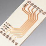
In the complex and rapidly evolving world of printed circuit board (PCB) manufacturing, the terminology can sometimes be overwhelming. However, understanding foundational concepts is crucial for designing reliable, high-performance electronics. One such critical concept is the PCB annular ring. An annular ring is the area of a لوحة نحاسية that surrounds a drilled and plated hole (via). This ring provides the necessary conductive surface area for electrical connections between different layers of a multi-layer board, or for component leads to be soldered securely.
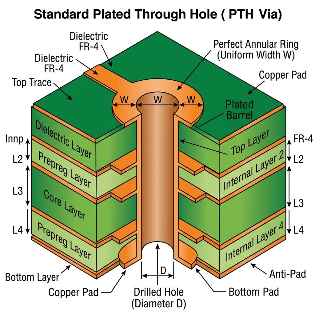
The width of the annular ring is determined by the difference between the diameter of the copper pad and the diameter of the drilled hole. A perfectly designed and manufactured annular ring will have a uniform width on all sides. When this width is sufficient, it ensures a strong and reliable electrical connection. However, due to manufacturing tolerances and the physical realities of the drilling process, perfectly centered holes are not always achieved. This is why understanding how to calculate, specify, and design these rings is paramount for any hardware engineer or PCB designer.
The Dangers of Annular Ring Breakout
When the drill bit wanders slightly from its intended target center during the manufacturing process, the resulting hole will be off-center relative to the copper pad. If this deviation is severe enough, the hole may actually breach the outer edge of the pad. This condition is known in the industry as a breakout. A breakout is a serious defect that can render a board completely useless.
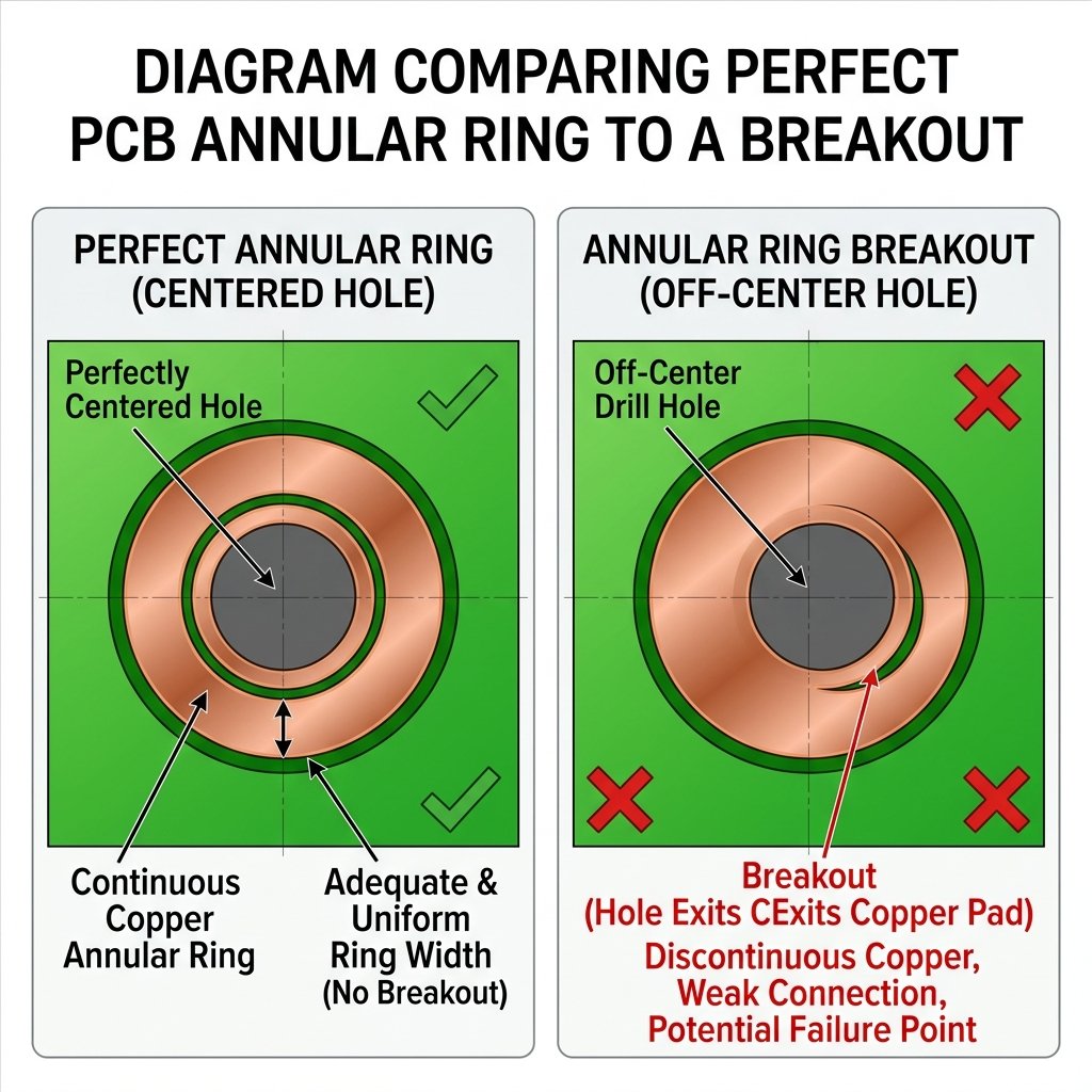
Breakouts are highly undesirable for several reasons. Firstly, they reduce the cross-sectional area of the copper connecting the via barrel to the trace on that specific layer. This can lead to increased electrical resistance and localized heating, particularly in high-current applications. Secondly, a breakout compromises the structural integrity of the via, making it more susceptible to failure under thermal or mechanical stress. During wave soldering or reflow, the thermal expansion of the board can cause a weak, broken-out connection to fail entirely, resulting in an open circuit. Finally, breakouts can lead to reliability issues in the field, which are notorious for being intermittent and incredibly difficult to debug. Preventing breakouts is therefore a top priority during the PCB design phase.
How to Design the Perfect Annular Ring
Follow these step-by-step instructions to ensure your PCB designs have adequate annular rings and are immune to breakouts during manufacturing.
Step 1: Understand Your Manufacturer’s Capabilities
The very first step in designing a reliable annular ring is to consult your chosen PCB manufacturer (fab house). Every manufacturer has specific tolerances for drill registration, which is the accuracy with which they can place a drilled hole relative to the printed copper image. This tolerance is usually expressed in mils (thousandths of an inch) or millimeters. You must know their minimum annular ring requirement for different copper weights and layer counts before you even begin routing your board. Failing to do so can lead to a board that is impossible to manufacture.
Step 2: Calculate the Minimum Pad Size
Once you know the minimum annular ring required by your fab house (e.g., 5 mils), and the finished hole size you need for your via or component lead (e.g., 10 mils), you can calculate the minimum pad size. It’s important to remember that the drill size is typically larger than the finished hole size by about 2-3 mils to account for the plating thickness. The formula for the minimum pad diameter is: Minimum Pad Size = (Minimum Annular Ring x 2) + Minimum Drill Size + Fabrication Allowance. Ensuring your pad size meets or exceeds this value is crucial.
Step 3: Account for Teardrops (Optional but Recommended)
To further reinforce the connection between the annular ring and the incoming trace, consider adding teardrops. Teardrops are extra copper added at the junction where a trace meets a pad. They provide a smooth transition and extra copper mass, which is incredibly helpful in preventing disconnects if the drill wanders slightly towards the trace exit point. Many modern EDA (Electronic Design Automation) tools can add teardrops automatically. While optional, teardrops are a sign of a robust and well-thought-out PCB design.
Step 4: Configure Design Rule Checks (DRC)
Humans make mistakes, which is why your PCB layout software has Design Rule Checks (DRC). You must input your manufacturer’s minimum annular ring specifications into your EDA tool’s DRC engine. Before generating your final manufacturing files (Gerbers or ODB++), run a full DRC pass. The software will automatically flag any vias or pads that violate your specified minimum annular ring, allowing you to correct them before sending the board to fabrication. This automated check is the final line of defense against poor annular ring design.
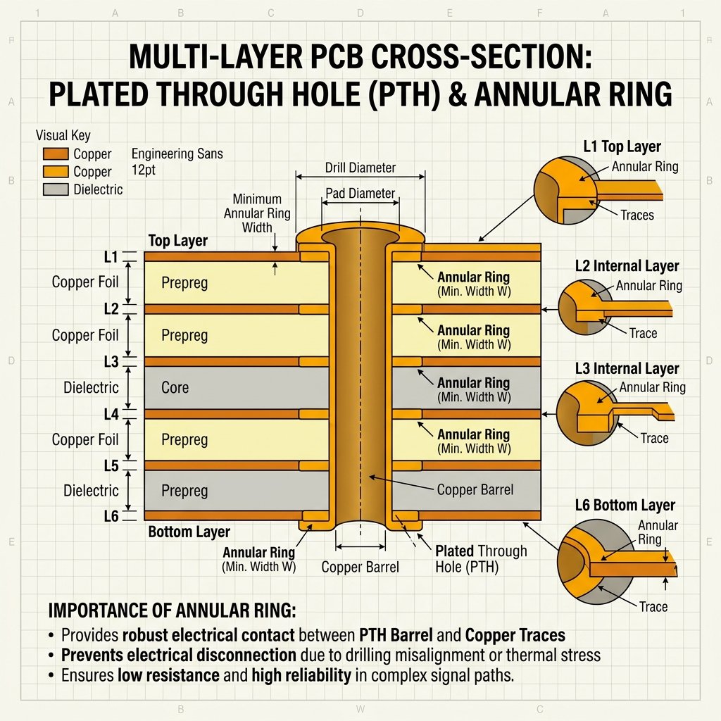
Best Practices for High-Reliability Boards
For applications where reliability is absolutely paramount—such as aerospace, medical devices, or automotive systems—meeting the bare minimum requirements is often not enough. In these scenarios, designers should strive for Class 3 compliance according to IPC standards (specifically IPC-6012). Class 3 boards have much stricter requirements for annular rings compared to Class 1 (general electronic products) or Class 2 (dedicated service electronic products). For instance, Class 3 typically does not allow any breakout whatsoever; the annular ring must be continuous and have a minimum width (often 1 mil or 2 mils depending on the layer and standard) even after accounting for all manufacturing tolerances and material variations.
When designing for Class 3, your pad sizes will naturally need to be larger, which can impact the overall كثافة التوجيه of your board. This is a classic engineering tradeoff: you are exchanging some space and density for significantly higher reliability. It is a price well worth paying for mission-critical hardware where failure is simply not an option. Always communicate openly with your manufacturer about your reliability goals to ensure their processes can support your design choices.
الأسئلة الشائعة
What is the IPC standard for annular rings?
The primary IPC standard that governs annular rings and other rigid PCB parameters is IPC-6012. It outlines the acceptability criteria for different classes of electronics (Class 1, 2, and 3), with varying strictness on allowable breakouts and minimum ring widths. Following IPC-6012 is generally recommended for any serious PCB design project.
Does the copper plating thickness affect the annular ring?
Yes, the copper plating thickness in the via barrel effectively reduces the final hole diameter. When calculating pad sizes, you must start with the raw drill size, not the finished plated hole size, because the physical annular ring is defined by the pad edge and the physical drilled hole edge before any plating is applied.
Can I use teardrops instead of a larger annular ring?
Teardrops are a great addition for reliability, but they do not technically increase the overall annular ring on all sides. They only reinforce the specific area where the trace connects to the pad. You must still meet the minimum annular ring requirement for the rest of the pad, but teardrops provide extra insurance against breakouts specifically at the critical trace junction.