Advanced PCB Via Filling Techniques for High Reliability Applications
When manufacturing high-density interconnect (HDI) printed circuit boards, managing vias effectively is a fundamental requirement. As electronic designs become increasingly denser and signal speeds continue to rise, understanding advanced pcb via filling techniques is no longer optional for high reliability applications. Proper via filling provides significantly improved structural integrity, enables better thermal management across the board, and prevents critical issues during the assembly and soldering processes.
The Importance of Advanced PCB Via Filling
Vias are the essential lifelines of multilayer boards, connecting different layers both electrically and thermally. However, leaving vias open and untreated can lead to severe problems such as solder wicking during the assembly phase. Solder wicking draws solder away from the intended joint, causing weak connections, open circuits, or short circuits on the opposite side of the board. While standard PCB manufacturing processes often include basic tenting (covering the via with solder mask) or plugging, high reliability applications demand much more robust and permanent solutions. This is where advanced PCB via filling comes into play. It ensures a completely solid, impermeable via structure that can withstand rigorous thermal cycling, mechanical stress, and harsh environmental conditions over the lifespan of the device.
Key Types of Via Filling Materials
Selecting the correct fill material is paramount to the success of the PCB. Conductive and non-conductive epoxy pastes are the two primary categories of materials used in advanced pcb via filling, each serving distinct engineering purposes.
Conductive Epoxy Fill
Conductive fills are specially formulated epoxy resins laced with metallic particles, most commonly silver or copper. These are utilized primarily when maximizing thermal and electrical conductivity through the board’s Z-axis is absolutely necessary. In applications like heavy power electronics or RF amplifiers, heat dissipation is critical. Using a conductive fill helps transport heat efficiently away from high-power components to internal ground planes or external heat sinks. However, it is important to note that conductive epoxies have a significantly different coefficient of thermal expansion (CTE) compared to the surrounding FR4 or high-frequency laminate. This CTE mismatch must be carefully managed by engineers to prevent stress fractures during operation.
Non-Conductive Epoxy Fill
Non-conductive epoxy is often the preferred and most common choice for standard high reliability boards. Despite its name, it still provides excellent structural support. Crucially, non-conductive epoxy is formulated to match the CTE of the surrounding advanced laminates much more closely than conductive pastes. By minimizing this CTE mismatch, you drastically reduce the risk of via barrel cracking during the thermal excursions of assembly and regular operation. Furthermore, HDI PCB design strategies often rely heavily on non-conductive fill followed by copper plating over the via, a technique known as Via-in-Pad Plated Over (VIPPO). This provides a perfectly flat, solderable surface for fine-pitch Ball Grid Array (BGA) components.
How Advanced PCB Via Filling is Performed
The process of via filling requires specialized precision equipment and strictly controlled manufacturing environments. Here is a general step-by-step breakdown of the advanced pcb via filling process.
-
Drilling and Initial Plating
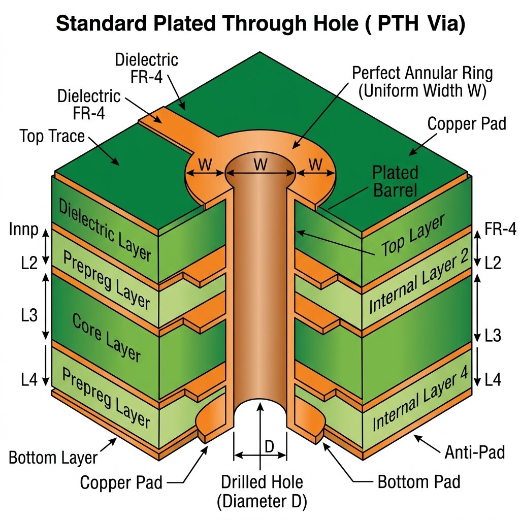
The initial step involves mechanically drilling or laser drilling the vias through the laminate. Once drilled, the vias undergo an electroless copper plating process followed by electrolytic plating to establish a robust conductive copper barrel wall inside the hole.
-
Surface Preparation
Before the filling paste is introduced, the board surface must be meticulously cleaned and prepped. Sometimes, a protective temporary film or tape is applied across the board surface to prevent the epoxy fill material from inadvertently adhering to the surface copper traces.
-
Vacuum Paste Filling
To ensure absolutely no air voids are trapped inside the via barrel, the epoxy paste is forced into the vias under a high vacuum environment. This is a highly critical aspect of advanced pcb via filling. Even microscopic voids can cause catastrophic failure during reflow soldering, as trapped moisture inside the void rapidly turns to steam and expands explosively.
-
Thermal Curing
The filled boards are placed in specialized convection ovens to cure the epoxy paste. The curing temperature profiles must be strictly controlled to ensure the epoxy hardens completely and uniformly without any outgassing or shrinking.
-
Planarization and Sanding
After curing, any excess hardened epoxy protruding from the vias is mechanically sanded or planarized using specialized planarization machines. This creates a perfectly smooth, flush surface across the entire printed circuit board.
-
Surface Overplating (For Via-in-Pad)
For advanced Via-in-Pad (VIPPO) designs, the newly planarized surface undergoes yet another copper plating cycle to deposit a solid cap of copper completely over the filled via. This provides a pristine, solid solderable pad directly on top of the via structure, which is essential for routing high pin-count BGAs effectively and minimizing signal inductance.
Applications Requiring Advanced Via Filling
Not every standard circuit board needs filled vias. However, certain demanding sectors absolutely cannot function reliably without these advanced manufacturing techniques:
- Aerospace and Defense: Boards subjected to extreme atmospheric pressure changes, massive temperature fluctuations, and severe physical vibration require the unmatched structural integrity provided by solid filled vias.
- Medical Devices: For implantable or life-critical medical equipment, high reliability is completely non-negotiable. Filled vias prevent chemical contamination and ensure consistent long-term electrical performance.
- Telecommunications and Data Centers: High-speed networking equipment utilizes incredibly dense HDI boards where Via-in-Pad technology is necessary to minimize signal path lengths, reduce parasitic capacitance, and maintain signal integrity at gigahertz frequencies.
To fully leverage these sophisticated manufacturing techniques, electronics designers must deeply understand the capabilities and limitations of their fabrication partners. Selecting the right PCB manufacturer with a proven, certified track record in advanced pcb via filling is just as critical to the product’s success as the circuit design itself.
Frequently Asked Questions about PCB Via Filling
Is conductive or non-conductive via fill better for HDI boards?
For the vast majority of applications, especially complex HDI boards using Via-in-Pad technology, non-conductive fill is far better due to its CTE (Coefficient of Thermal Expansion) closely matching the surrounding FR4 laminate. This drastically reduces the risk of copper barrel cracking during thermal cycling. Conductive fill is typically reserved for very specific, niche cases requiring extreme thermal transfer away from hot components.
What exactly happens if there are air voids in the via fill?
Air voids trap both air and ambient moisture. During the extreme high heat of the assembly reflow soldering process, this trapped moisture rapidly turns to steam and expands with immense pressure. This can potentially blow out the side of the via, delaminate the internal layers of the board, or crack the copper plating, completely ruining the PCB. Advanced vacuum filling processes are specifically used to prevent this exact scenario.
Does via filling add significant cost to PCB manufacturing?
Yes, advanced pcb via filling requires several additional, time-consuming manufacturing steps including vacuum filling, high-temperature curing, mechanical planarization, and often extra copper plating cycles. This increases both the manufacturing lead time and the overall cost of the bare board, but it is an absolutely necessary investment for high reliability and dense HDI designs.