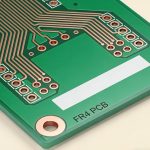
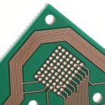
In the highly competitive world of electronics, minimizing production costs without sacrificing quality is paramount. Improving overall PCB (Printed Circuit Board) manufacturability is one of the most effective ways to achieve this balance. Manufacturability, often referred to as Design for Manufacturing (DFM), ensures that a PCB can be produced easily, reliably, and cost-effectively. In this comprehensive guide, we will explore actionable strategies, essential guidelines, and best practices to optimize your PCB designs for manufacturing and assembly, ultimately driving down costs and accelerating time-to-market. When companies prioritize manufacturability early in the design cycle, they significantly reduce the risk of unexpected production delays, enabling faster product launches and improved profitability across the entire hardware lifecycle.
Why PCB Manufacturability Matters
PCB manufacturability directly impacts both the production timeline and the bottom line. Complex designs with tight tolerances, unusual materials, or excessive layers increase the likelihood of manufacturing defects, leading to lower yields and higher scrap rates. By designing with manufacturability in mind from the outset, engineers can streamline the fabrication process, reduce the need for manual interventions, and minimize costly revisions. This proactive approach not only lowers production costs but also enhances the overall reliability and performance of the final product. Every step taken to improve manufacturability helps in minimizing manual touch-ups during the assembly process, lowering labor costs and ensuring consistent, high-quality output for large volume production runs.
Key Strategies for Improving Manufacturability
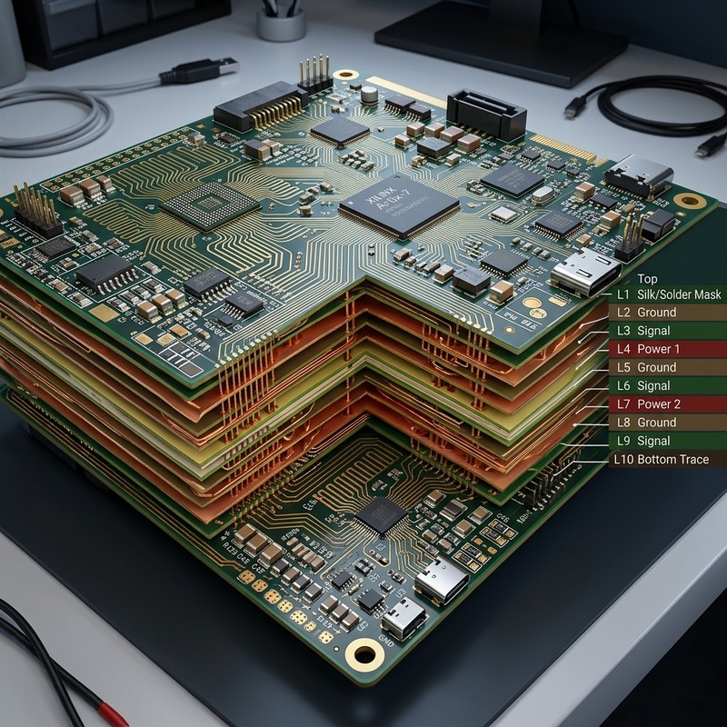
To optimize your PCB designs for manufacturing, consider implementing the following key strategies. These practices address common challenges in fabrication and assembly, ensuring a smoother production cycle. It is crucial to remember that decisions made during the layout phase dictate the efficiency of both bare board fabrication and PCBA (Printed Circuit Board Assembly).

1. Optimize Component Placement and Routing
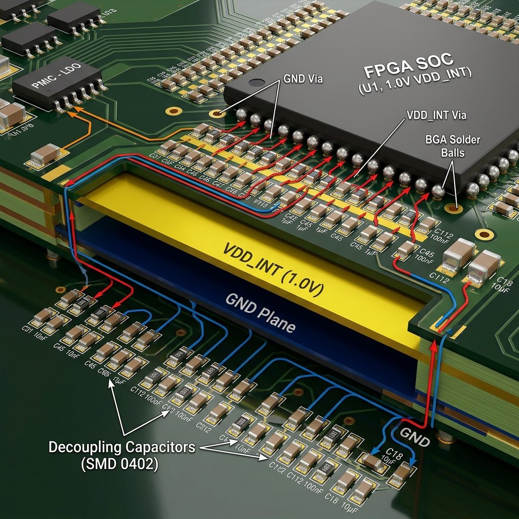
Proper component placement is crucial for efficient assembly and reliable performance. Group related components together to minimize trace lengths and reduce signal interference. Ensure adequate spacing between components to facilitate automated assembly and inspection processes, such as Automated Optical Inspection (AOI) and X-ray inspection. Additionally, consider the thermal implications of component placement; place heat-generating components near the edges of the board or strategically position them to maximize airflow. Good routing also minimizes the risk of crosstalk and electromagnetic interference (EMI). For more detailed insights on thermal management, read about كيفية تحسين صب النحاس في لوحات الدوائر المطبوعة (PCB) لتحقيق تبديد حراري أفضل.
2. Standardize Hole Sizes and Pad Designs
Using a wide variety of drill hole sizes increases manufacturing time and costs, as it requires frequent tool changes during the drilling process. Standardize hole sizes whenever possible to streamline fabrication. Work with your manufacturer to understand their standard drill sizes and design accordingly. Similarly, adhere to standard pad designs to ensure reliable soldering during assembly. Proper pad design prevents common defects such as tombstoning, solder bridging, and voiding, which can be costly to repair. For essential guidelines, review these نصائح أساسية لتصميم نقاط التوصيل على لوحات الدوائر المطبوعة (PCB) من أجل تجميع موثوق بالتقنية السطحية (SMT).
3. Implement Proper Thermal Reliefs and Clearances
Connecting large copper planes directly to component pads can act as a heat sink during soldering, leading to cold solder joints or incomplete wetting. Implementing thermal reliefs on these connections ensures proper heat concentration at the pad, improving soldering quality and reliability. Learn more about تطبيق التبريد الحراري للوحات الدوائر المطبوعة (PCB) لتحسين جودة اللحام. Furthermore, maintaining appropriate clearances between traces, pads, and solder mask is essential to prevent electrical shorts and manufacturing defects. Understanding لماذا يُعد الفراغ بين قناع اللحام ولوحة الدوائر المطبوعة (PCB) عاملاً مهمًا في تحقيق عملية لحام خالية من العيوب is critical for robust designs. Good clearance rules also help prevent issues during the solder mask application process.
How to Implement DFM (Design for Manufacturing) Checks
A step-by-step guide to incorporating Design for Manufacturing checks into your PCB design workflow to ensure cost-effective and reliable production.
Step 1: Set Up Design Rules
Step 2: Run Automated DFM Analysis
Step 3: Review and Resolve Errors
Step 4: Collaborate with the Manufacturer
الأسئلة الشائعة
What is PCB manufacturability?
PCB manufacturability, also known as Design for Manufacturing (DFM), refers to the practice of designing a printed circuit board in a way that makes it easy, reliable, and cost-effective to produce and assemble without compromising on functional performance.
How does DFM reduce production costs?
DFM reduces production costs by minimizing the likelihood of manufacturing defects, reducing scrap rates, streamlining fabrication processes, and eliminating the need for costly design revisions and manual rework. It optimizes the use of materials and standardizes components, leading to economies of scale.
Why is it important to consult with the manufacturer early in the design process?
Consulting with the manufacturer early allows engineers to understand the specific capabilities and constraints of the production facility. This ensures the design is optimized for their processes, preventing delays, unexpected costs, and ensuring that the final product meets all quality standards.