In the ever-evolving world of electronics, the demand for smaller, faster, and more reliable devices is constant. This demand places immense pressure on printed circuit board (PCB) designers and manufacturers to maximize space and efficiency. One of the most critical technologies enabling this miniaturization in complex multi-layer PCBs is the use of buried vias. In this comprehensive guide, we will explore buried via applications, their manufacturing process, and how they contribute to high-density interconnect (HDI) designs.
What are Buried Vias?
A buried via is a copper-plated hole that connects two or more internal layers of a multi-layer PCB but does not extend to the top or bottom outer layers. Because they are completely encapsulated within the board, they are invisible from the outside. This is in contrast to through-hole vias, which traverse the entire thickness of the board, and blind vias, which connect an outer layer to one or more inner layers but do not go all the way through.
The primary advantage of buried vias is that they free up valuable routing space on the surface and other internal layers. By restricting the via to only the necessary layers, designers can route traces over or under the buried via on other layers, significantly increasing the routing density of the board. This is particularly crucial in designs utilizing a 10 layer PCB stackup or higher, where routing space is at a premium.
Key Applications of Buried Vias
Buried vias are indispensable in modern electronics, finding applications in various high-performance devices.
1. High-Density Interconnect (HDI) Boards
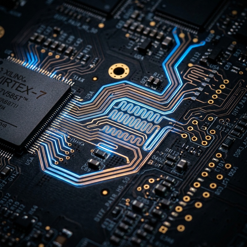
The most prominent application of buried vias is in HDI PCBs. These boards are characterized by high wiring density per unit area, fine lines and spaces, and small via diameters. Buried vias, often used in conjunction with microvias and blind vias, are the backbone of HDI technology. They allow for the complex routing required by high-pin-count components like Ball Grid Arrays (BGAs) and complex processors. If you want to understand why smart devices require an HDI PCB stackup for compact designs, buried vias are a major part of the answer.
2. Telecommunications and Networking Equipment
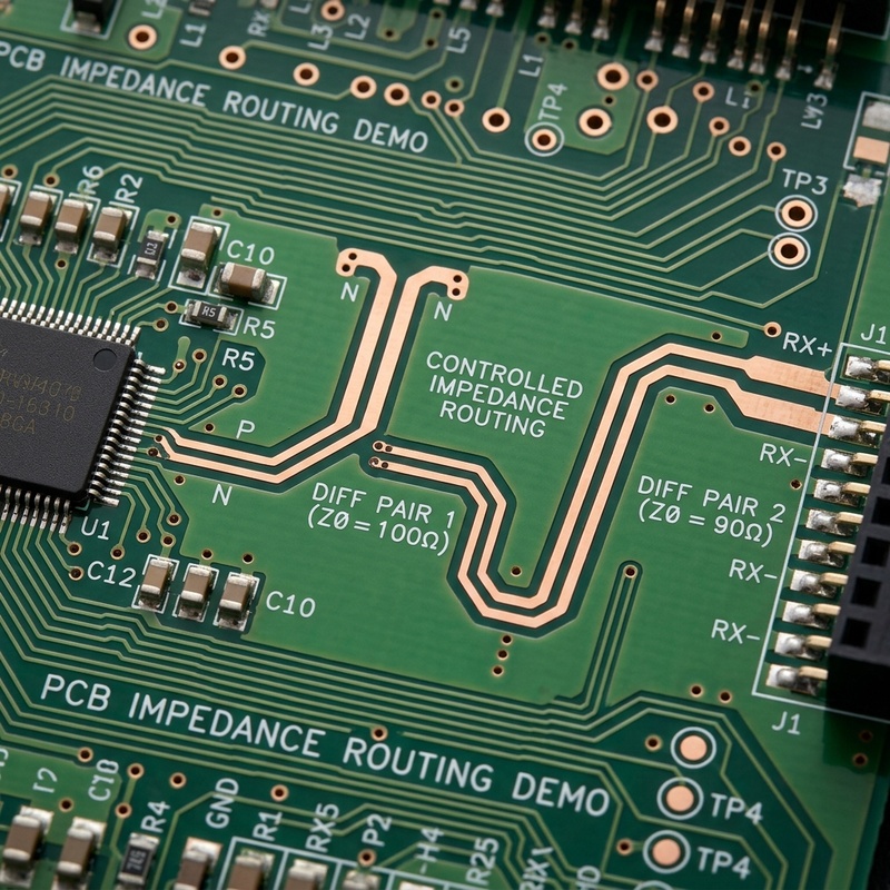
High-speed routers, switches, and base stations require PCBs capable of handling high-frequency signals with minimal loss and interference. Buried vias help in creating shorter signal paths, reducing parasitic capacitance and inductance, which is vital for maintaining signal integrity. This is closely related to essential rules for high-speed PCB stackup configuration.
3. Aerospace and Defense
Reliability is paramount in aerospace and defense applications. Buried vias, being protected within the internal layers of the PCB, are less susceptible to environmental factors like moisture and mechanical stress compared to through-hole vias. They provide robust internal connections essential for mission-critical systems.
4. Medical Devices
From portable diagnostic equipment to implantable devices, the medical industry demands extreme miniaturization without compromising reliability. Buried vias enable the creation of highly compact and reliable PCBs that fit into the stringent form factors required by modern medical technology.
The Manufacturing Process of Buried Vias
The fabrication of PCBs with buried vias is more complex and time-consuming than standard through-hole boards, which typically increases the manufacturing cost. Here is a simplified overview of the process:
How to Manufacture Buried Vias
A step-by-step guide to the manufacturing process of buried vias in multi-layer PCBs.
-
Inner Layer Preparation:
The process begins by manufacturing the inner core layers that will contain the buried via. These layers are drilled, plated, and etched just like a standard two-layer PCB.
-
Drilling the Buried Via:
Holes are drilled into the prepared inner layers where the buried vias are required.
-
Plating:
The drilled holes are then plated with copper to establish the electrical connection between the designated inner layers.
-
Filling (Optional but recommended):
To prevent resin from flowing into the via during subsequent lamination steps and to ensure a flat surface, the buried vias are often filled with a conductive or non-conductive epoxy.
-
Lamination:
The inner layers containing the buried vias are then stacked with the remaining layers of the PCB (prepreg and outer copper foils) and laminated together under heat and pressure.
-
Final Processing:
The board undergoes the standard final processing steps, including drilling for through-hole components, outer layer etching, solder mask application, and surface finish.
Design Considerations for Buried Vias
When incorporating buried vias into a design, several factors must be considered to ensure manufacturability and reliability:
- Aspect Ratio: The aspect ratio (depth-to-diameter) of the buried via must be kept within the manufacturer’s capabilities to ensure reliable plating.
- Layer Pairing: Buried vias are typically drilled through a core material, so they must connect adjacent layers separated by a core. Connecting arbitrary internal layers requires sequential lamination, significantly increasing cost and complexity. Proper advanced routing strategies for 8 layer PCB stackup designs (or any multi-layer design) are necessary.
- Cost vs. Benefit: The addition of buried vias increases the fabrication cost. Designers must weigh this cost against the benefits of increased routing density and smaller board size.
Frequently Asked Questions (FAQ)
What is the difference between a blind via and a buried via?
A blind via connects an outer layer of the PCB to one or more inner layers but does not go all the way through the board. A buried via connects two or more inner layers and is completely enclosed within the board, making it invisible from the outside.
Are buried vias expensive?
Yes, PCBs with buried vias are more expensive to manufacture than standard multi-layer boards. The process requires extra drilling, plating, and lamination steps, which increases both time and material costs.
When should I use buried vias?
Buried vias should be used when you have a high-density design with limited routing space, such as in complex HDI boards, or when you need to improve signal integrity by minimizing via stub length in high-speed applications.
Conclusion
Buried vias are a powerful tool in the arsenal of PCB designers, enabling the creation of compact, high-performance electronics. While they add complexity and cost to the manufacturing process, their ability to drastically improve routing density makes them essential for modern HDI designs and complex multi-layer boards. By understanding their applications, manufacturing process, and design considerations, engineers can effectively leverage buried vias to push the boundaries of electronic design.