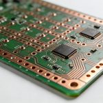
In the ever-evolving landscape of modern electronics, miniaturization and high performance are paramount. The demand for compact yet powerful devices has propelled High-Density Interconnect (HDI) Printed Circuit Boards (PCBs) to the forefront of manufacturing technology. At the heart of this revolution lies microvia technology, a critical innovation that enables the intricate, high-density routing required by today’s advanced electronic products.
What is Microvia Technology?
Microvias are microscopic holes drilled into a PCB, typically using advanced laser technology, to connect different layers of the board. Unlike traditional mechanical drilling, laser drilling allows for incredibly small diameters—often less than 150 micrometers. This precision makes microvias indispensable in HDI PCBs, where space is at a premium and routing density is exceptionally high.
The implementation of microvias allows designers to pack more functionality into a smaller footprint. This is especially evident when considering why smart devices require an HDI PCB stackup for compact designs, as the ability to route complex signals without consuming excessive board space is critical for smartphones, wearables, and IoT devices.
Types of Microvias
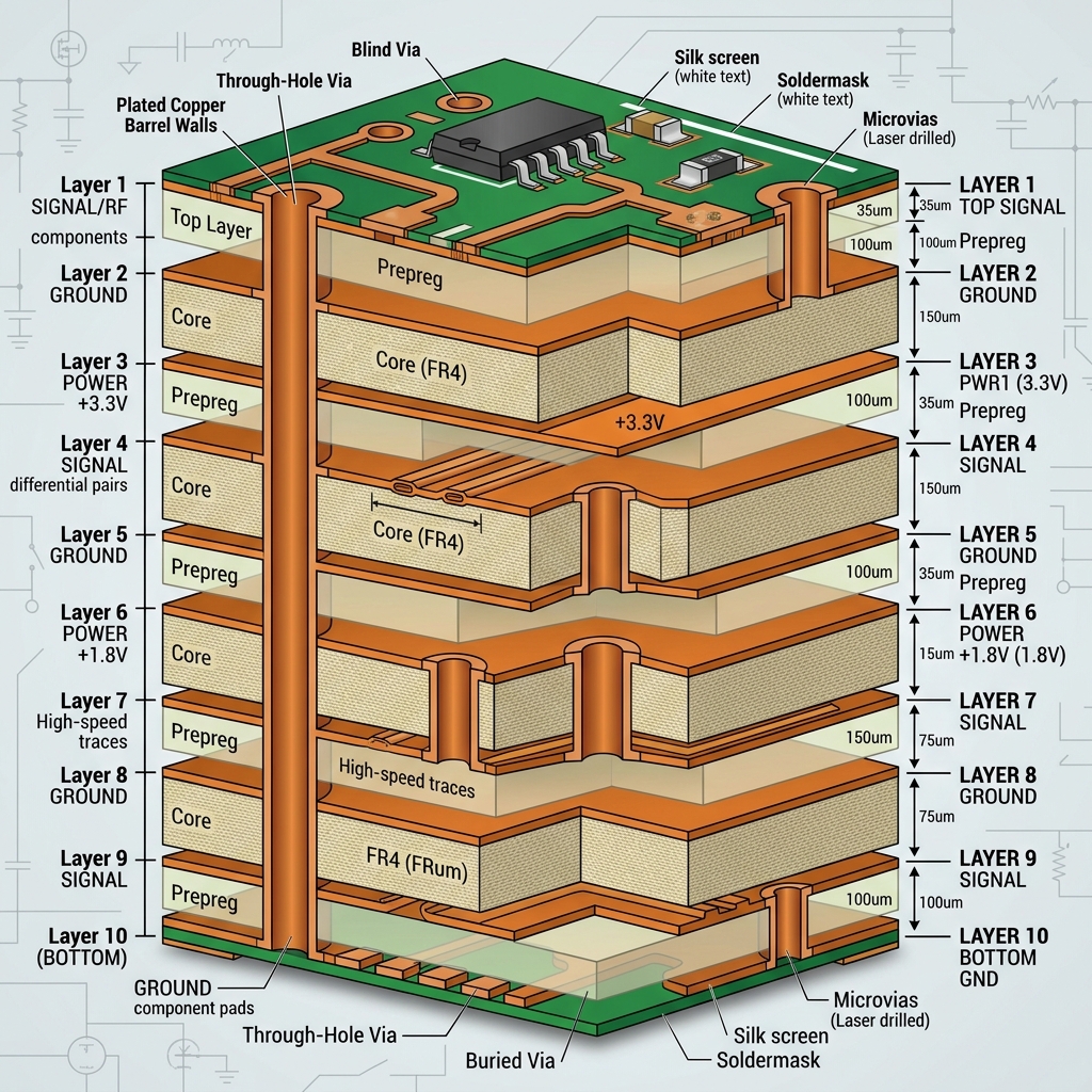
Understanding the different types of microvias is essential for optimizing PCB designs. The three primary types are:
- Blind Microvias: These connect an outer layer of the PCB to one or more inner layers but do not pass entirely through the board. They are highly effective for increasing routing density on the outer layers.
- Buried Microvias: Connecting only internal layers, buried microvias are completely hidden from the outside. They free up valuable real estate on the board’s surface for component placement.
- Stacked and Staggered Microvias: In complex multi-layer boards, microvias can be stacked directly on top of each other or staggered across layers to create continuous electrical pathways through the HDI stackup.
How Microvia Technology Enhances HDI PCB Design
How to Leverage Microvias for Optimal HDI PCB Design
A step-by-step approach to integrating microvias into your HDI PCB layout for maximum performance and space efficiency.
Step 1: Determine the Required Layer Count
Start by evaluating the complexity of your circuit. Decide whether you need a complex multi-layer design or if a simpler stackup will suffice. For guidance, refer to a step by step guide to designing a 4 layer PCB stackup to understand foundational layering strategies.
Step 2: Define Microvia Structures
Choose the appropriate mix of blind, buried, and stacked microvias based on your routing needs. Ensure that your manufacturer supports the chosen aspect ratios and drilling techniques.
Step 3: Optimize Trace Widths and Spacing
With microvias saving space, you can fine-tune your trace dimensions. Carefully consider your power requirements, such as calculating the ideal PCB trace width for high current applications, to ensure reliable power delivery alongside high-density signal routing.
Step 4: Refine Pad Design
Microvias are often placed directly within component pads (via-in-pad) to maximize space savings, particularly for fine-pitch BGA components. Review essential PCB pad design tips for reliable SMT assembly to ensure that your via-in-pad implementation does not compromise solder joint integrity.
The Impact of Microvias on Signal Integrity and Reliability
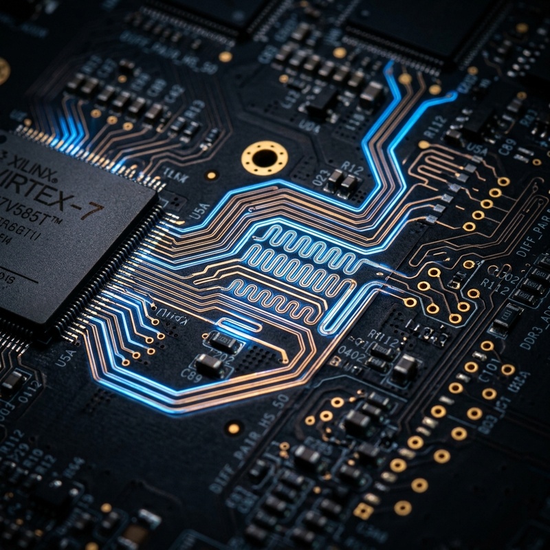
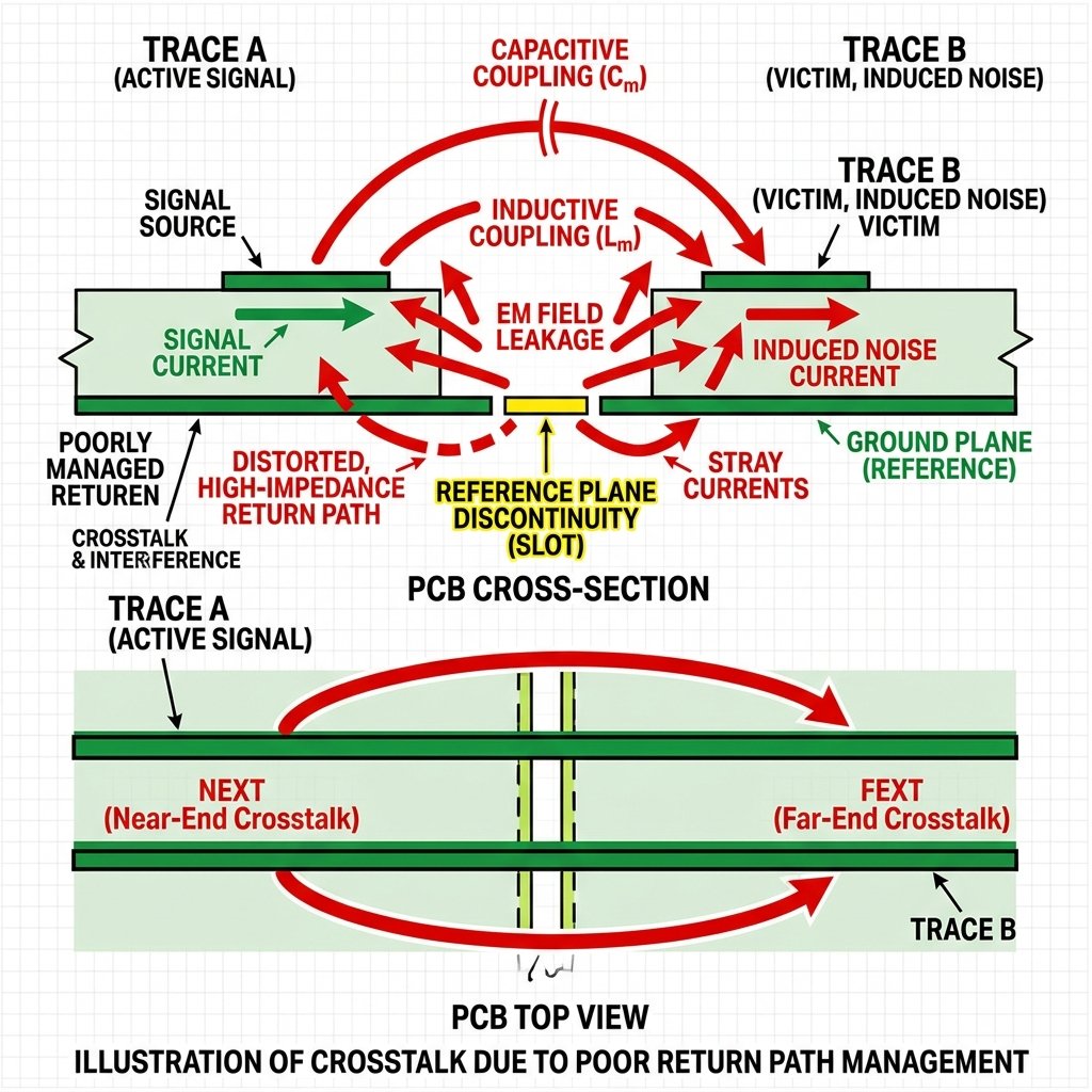
Beyond simple space-saving, microvia technology significantly improves electrical performance. The short length and small diameter of microvias result in lower parasitic capacitance and inductance compared to standard through-hole vias. This reduction is critical in high-speed digital circuits and RF applications, where signal degradation must be minimized. The tighter routing enabled by microvias also helps in maintaining controlled impedance and reducing electromagnetic interference (EMI).
However, the manufacturing process for microvias demands rigorous quality control. The laser drilling process must be precise, and the subsequent copper plating must be uniform to prevent voids and ensure a reliable electrical connection. Advanced techniques, such as copper-filled microvias, are often employed to enhance thermal management and provide a flat surface for via-in-pad assembly.
Frequently Asked Questions
What is the main advantage of microvia technology in HDI PCBs?
The primary advantage is miniaturization. Microvias allow for significantly higher routing densities, enabling designers to fit complex circuits into much smaller and lighter form factors, which is essential for modern portable electronics.
Can microvias handle high current?
Individual microvias have limited current-carrying capacity due to their small size. However, designers often use multiple microvias in parallel to handle higher currents safely while maintaining the benefits of HDI design.
Is microvia manufacturing more expensive than traditional vias?
While the specialized laser drilling and plating processes for microvias can increase the cost per layer, the overall cost of the PCB may decrease. By using microvias, designers can often reduce the total number of layers or the overall board size, offsetting the specialized manufacturing costs.
Conclusion
Microvia technology is not just an incremental improvement; it is a foundational pillar of modern electronics design. By enabling the creation of High-Density Interconnect PCBs, microvias empower engineers to push the boundaries of miniaturization, performance, and functionality. As smart devices continue to become smaller, faster, and more capable, the reliance on advanced microvia structures will only continue to grow, cementing their role as a critical driver of innovation in the PCB industry.