Understanding the PCB Copper Plating Process in Manufacturing
When diving into the complex world of modern electronics production, understanding the pcb copper plating process is an absolute necessity. Copper plating is the fundamental backbone for establishing reliable electrical connectivity within a printed circuit board. Without a solid, properly deposited layer of copper to carry the signals and power throughout the various substrate layers, today’s sophisticated electronic devices simply would not function. This article will explore the nuances of copper plating, the chemical and physical mechanisms behind it, and why mastering this technique is so critically important to the overall PCB manufacturing process.
Why is Copper Plating Necessary?
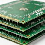
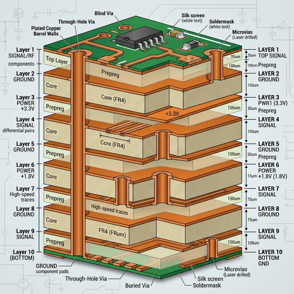
Printed circuit boards typically consist of insulating dielectric materials, such as FR4 fiberglass, which are laminated with thin layers of copper foil. However, to create essential electrical connections between the top, bottom, and internal layers, tiny holes must be drilled through the board. These drilled holes, commonly known as vias, are initially non-conductive because they expose the raw fiberglass substrate.
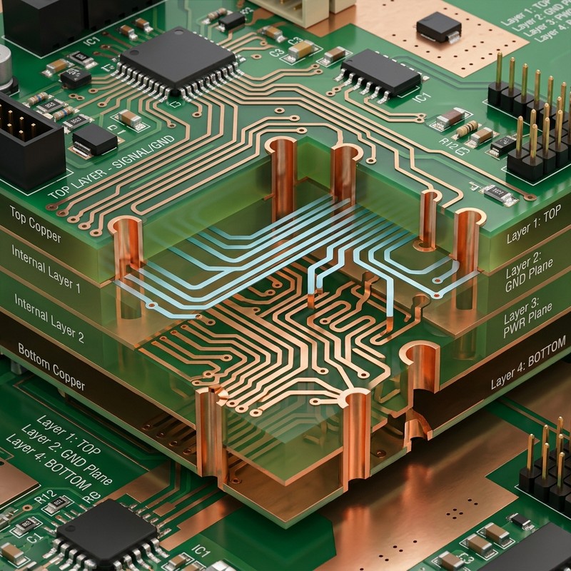
The copper plating process is responsible for depositing a highly conductive layer of copper directly onto the non-conductive walls of these drilled holes, thereby enabling electronic signals to travel freely from one layer to another. This interconnectivity is especially critical when dealing with a complex multilayer PCB, where internal routing demands robust vertical interconnect access. In addition to making the vias conductive, the copper plating stage can also selectively increase the thickness of the surface copper traces, allowing them to carry higher currents without overheating or suffering from voltage drops.
Step-by-Step Guide to the Copper Plating Process
The comprehensive process of copper plating involves a meticulously controlled sequence of chemical baths and electrical treatments designed to ensure an even, highly reliable deposition. Here is a detailed breakdown of the standard manufacturing procedure.
Step 1: Desmear and Hole Cleaning
Immediately after drilling, the holes usually contain a resin smear caused by the immense heat of the drill bit melting the epoxy substrate. A highly aggressive chemical desmear process, often involving potassium permanganate, is applied to dissolve and remove this resin. This step also subtly roughens the hole walls, generating a micro-textured surface that ensures the subsequent chemical layers will anchor and adhere properly to the substrate.
Step 2: Electroless Copper Deposition
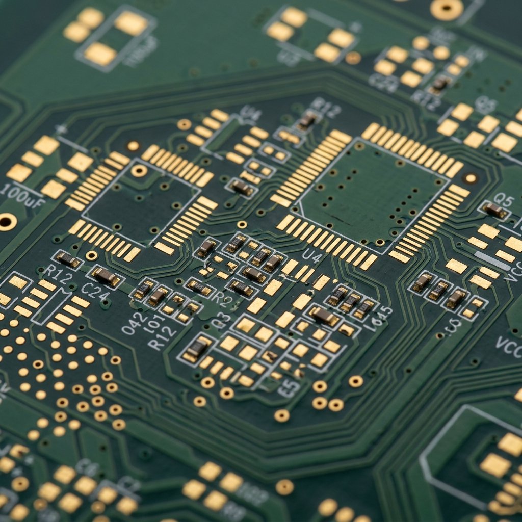
Because the fiberglass substrate exposed inside the hole is an inherent electrical insulator, traditional electroplating cannot begin immediately. First, an autocatalytic chemical process known as electroless copper deposition is employed. By immersing the boards in a specialized bath, a microscopic layer of copper is chemically precipitated onto all exposed surfaces, including the hole walls. This critical step creates a continuously conductive base layer, setting the stage for thicker plating.
Step 3: Electrolytic Copper Plating
Once the initial conductive layer is successfully established, the panel is submerged in a large electrolytic bath containing a solution of copper sulfate and sulfuric acid. An electrical direct current (DC) is applied through the system, causing positively charged copper ions to migrate from solid copper anodes and plate evenly onto the board and deep inside the vias. This step builds the copper to the required physical thickness, providing excellent electrical conductivity for robust through-hole technology component mounting and thermal dissipation.
Step 4: Rinsing and Drying
Finally, the plated boards are thoroughly rinsed through multiple cascading water stations to remove any residual, highly acidic plating chemicals. They are then fully dried. After this critical phase is complete, the panels are ready for the next stages of manufacturing, such as outer layer photo-imaging or applying a final protective surface finish to prevent oxidation.
Challenges Encountered in Copper Plating
While the overall process is well understood by industry professionals, it is certainly not without its technical challenges. One of the primary issues engineers face is achieving uniform plating thickness, especially in high aspect ratio holes—instances where the hole is exceptionally deep compared to its narrow diameter. Uneven plating or “dog-boning” can lead to dangerously thin copper in the center of the via barrel, which might result in weak connections or complete failure of the via under intense thermal stress during component soldering.
To combat this, manufacturers use sophisticated organic plating additives (such as brighteners, levelers, and carriers) and tightly controlled fluid dynamics within the plating baths. These modern innovations ensure that the copper ions reach deep into these challenging holes, providing a reliable, robust, and uniform conductive barrel that meets stringent quality standards.
Frequently Asked Questions
Why is copper used instead of other metals like gold or silver?
Copper offers an exceptional, virtually unbeatable balance of high electrical conductivity, reasonable material cost, and excellent physical workability. While silver and gold are marginally more conductive, their prohibitively high cost prevents their use for the bulk of the main circuit traces. Thus, understanding the pcb copper properties clarifies why it has remained the steadfast industry standard for decades.
What is the functional difference between electroless and electrolytic plating?
Electroless plating is a purely chemical, autocatalytic process that deposits a very thin layer of copper on non-conductive surfaces without requiring any external electricity. Electrolytic plating, on the other hand, strictly requires an electrical current to drive the continuous deposition of a much thicker, more structurally robust layer of copper on top of a pre-existing conductive base.
How thick is the standard copper plating inside a via?
The standard, widely accepted thickness for copper plating inside a via barrel is typically around 20 to 25 micrometers (approximately 0.8 to 1.0 mil). However, this can vary significantly based on specific, custom design requirements, especially for specialized boards that need to handle high power currents or endure severe thermal cycling in harsh environments like aerospace or automotive applications.