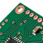
In the ever-evolving world of electronics manufacturing, the demand for smaller, faster, and more efficient devices continues to drive innovation in printed circuit board (PCB) design. One of the key techniques that has emerged to meet these demands is Via in Pad technology. This approach allows designers to achieve higher component densities and better electrical performance, especially when dealing with complex components like Ball Grid Arrays (BGAs). However, like any manufacturing technique, it comes with its own set of advantages and limitations.
What is Via in Pad Technology?
Traditional PCB design involves placing vias—small conductive pathways that connect different layers of the board—next to component pads, connected by a short trace. This method takes up valuable board space. Via in Pad technology, on the other hand, places the via directly underneath the component pad. The via is typically filled with conductive or non-conductive epoxy and then plated over to create a flat, solderable surface.
This technique is particularly useful for routing fine-pitch BGAs and high-density interconnect (HDI) boards, where space is at an absolute premium. If you are exploring the intricacies of modern board design, you might want to learn Why Smart Devices Require an HDI PCB Stackup for Compact Designs.

Advantages of Via in Pad

Space Savings and Higher Density
The most obvious benefit of placing a via directly in the pad is the significant space savings. By eliminating the need for dog-bone routing or external traces to connect pads to vias, designers can pack more components into a smaller area. This is essential for modern smartphones, wearables, and compact IoT devices.
Improved Signal Integrity
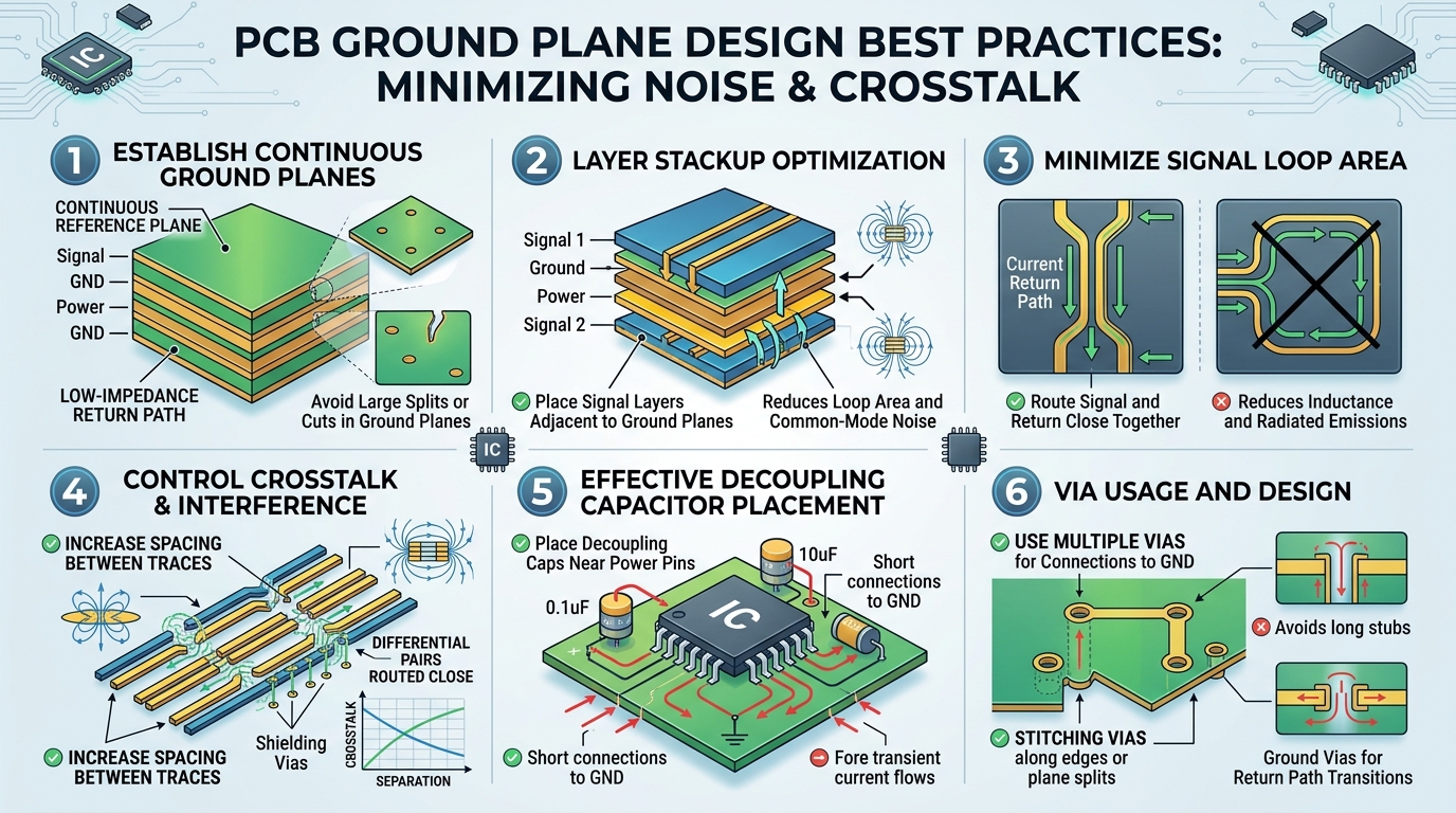
In high-speed electronic circuits, the length of the signal path is critical. Every millimeter of trace can introduce inductance, capacitance, and resistance, potentially degrading signal quality. By placing the via directly under the pad, the signal path is minimized, reducing parasitic inductance and capacitance. This leads to cleaner, faster signal transmission, which is crucial for high-frequency applications.
Enhanced Thermal Management
Vias can act as excellent thermal conduits, transferring heat away from power-hungry components. When a via is placed directly within a component pad, it can draw heat directly from the component’s underside and dissipate it into internal copper planes or the opposite side of the board. Proper thermal management often goes hand in hand with learning How to Optimize PCB Copper Pour for Better Thermal Dissipation.
Limitations and Challenges
Increased Manufacturing Complexity and Cost
The process of creating a via in pad is significantly more complex than standard via creation. The vias must be drilled, plated, filled with epoxy, planarized (sanded flat), and then over-plated. Each of these extra steps adds time and cost to the manufacturing process. For cost-sensitive projects, this added expense might be hard to justify.
Potential for Solder Wicking
If the via in pad is not properly filled and plated flat, the hole can act as a capillary tube during the reflow soldering process. Solder intended for the component pad can be drawn down into the via, leaving insufficient solder on the pad and potentially causing weak or open joints. Understanding Essential PCB Pad Design Tips for Reliable SMT Assembly is vital to prevent such manufacturing defects.
Design Constraints
Using via in pad technology requires strict adherence to design rules. The aspect ratio of the via, the type of fill material, and the thickness of the over-plating must all be carefully calculated. For designers used to traditional through-hole techniques, this requires a learning curve. If you are transitioning from older methods, reviewing guidelines on Selecting the Right PCB Hole Size for Through Hole Components can provide a solid foundation for understanding via dimensions.
How to Implement Via in Pad (Step-by-Step Guide)
Implementing Via in Pad
A standard process for designing a via in pad on a PCB.
1. Determine the Via Size
Calculate the required drill size and pad diameter based on your current handling and manufacturing capabilities.
2. Select the Fill Material
Choose between conductive or non-conductive epoxy fill depending on thermal and electrical requirements.
3. Apply the Over-Plating
Ensure the via is plated over smoothly to create a flat, coplanar surface for the component to be soldered onto.
4. Verify with DRC
Run a comprehensive Design Rule Check (DRC) to ensure all clearances and constraints are met.
Frequently Asked Questions
When should I use via in pad technology?
It is highly recommended when dealing with high-density designs, specifically for fine-pitch BGAs (0.5mm pitch or less), or when superior signal integrity and thermal dissipation are critical.
Is conductive or non-conductive epoxy better for filling vias?
Non-conductive epoxy is often preferred because it expands less during the thermal stress of reflow soldering, reducing the risk of cracked via plating. Conductive epoxy is primarily used when extreme thermal or electrical conductivity is required through the via itself.
Does via in pad increase the cost of my PCB?
Yes, the additional manufacturing steps like filling, planarizing, and over-plating add to the overall fabrication cost and turnaround time.
Conclusion
Via in pad technology is an indispensable tool in the modern electronic designer’s arsenal. While it introduces additional manufacturing complexities and costs, its benefits in terms of space savings, signal integrity, and thermal performance are often well worth the investment. By understanding its advantages and limitations, engineers can make informed decisions to create robust, high-performance printed circuit boards.