When and How to Apply Back Drilling in High Speed PCBs
In the rapidly evolving realm of advanced electronics and telecommunications, maintaining immaculate signal integrity across complex printed circuit boards is paramount. As data transfer rates continually push boundaries, engineers are faced with overcoming physical limitations that were once considered negligible. One critical, yet sometimes overlooked, technique for achieving this in multi-layer boards is back drilling. Understanding exactly when and how to apply back drilling in high-speed PCBs can ultimately be the deciding factor between a fully functional, high-performance product and a costly, time-consuming failure during the testing phase. This comprehensive, deep-dive guide will meticulously explore the nuances of this essential manufacturing process, helping you optimize your sophisticated designs for peak performance.
Understanding the Basics: What is Back Drilling?
Back drilling, frequently referred to in the industry as controlled depth drilling (CDD), is a precise manufacturing process used to meticulously remove the unused, extraneous portion—or stub—of a plated through-hole (PTH) via. In standard PCB manufacturing, a via goes all the way through the board, even if the signal only needs to travel from layer 1 to layer 3 of a 10-layer board. The remaining portion from layer 3 down to layer 10 acts as a stub.
These seemingly harmless stubs can essentially act as tiny antennas within your board. At higher frequencies, they cause severe signal reflections, resonance, and overall signal degradation, significantly increasing the bit error rate (BER). By physically eliminating the stub through a secondary drilling pass, designers and fabricators can significantly improve the signal integrity of their high-speed circuits, ensuring a much cleaner eye diagram and reliable data transmission.
Strategic Implementation: When and How to Implement Back Drilling
Determining when and how to systematically apply this technique requires a careful, analytical approach to your circuit’s specific operating frequencies and the physical constraints of your PCB stackup. It is typically recommended when your signal speeds begin to exceed 3 Gbps (Gigabits per second). However, if your design features unusually tight timing margins or utilizes an especially thick backplane, tighter margins may necessitate back drilling at even lower speeds.
For more foundational knowledge on high-speed routing strategies, you can review our comprehensive high-speed PCB design guidelines, which detail various complementary techniques for maintaining signal fidelity across increasingly complex multi-layer stacks.
How to Apply Back Drilling in Your PCB Design
Successfully incorporating back drilling requires coordination between the design engineer and the fabrication house. Follow these detailed, sequential steps to seamlessly integrate back drilling into your high-speed PCB manufacturing process.

Step 1: Identify Critical High-Speed Signals
Start your optimization journey by carefully analyzing your schematic and identifying the specific high-speed nets that are most susceptible to signal degradation. These are typically your high-speed serial links (like PCIe, SerDes, or 10G Ethernet), high-speed clocks, and fast memory interfaces (like DDR4 or DDR5). Performing a thorough, simulation-driven signal integrity analysis will help pinpoint exactly which vias in the layout are causing problematic reflections and require stub removal.
Step 2: Determine Maximum Stub Length Requirements
Once you’ve identified the critical nets, calculate the maximum allowable stub length for your specific operating frequency. As a general rule of thumb in high-speed design, the stub length should ideally be kept to less than one-tenth of the highest frequency component’s wavelength. The shorter the stub, the better the resulting signal integrity will be. Your simulation tools can help validate these calculations.
Step 3: Define Precise Back Drill Parameters in CAD
In your chosen PCB layout software (such as Altium Designer, Cadence Allegro, or Mentor Graphics), accurately configure the properties of the vias that require back drilling. You must specify the starting layer, the crucial ending layer (the layer just before the signal trace makes its connection), and the drill bit size. The back drill bit is usually sized slightly larger than the original PTH drill bit to ensure the complete removal of the copper plating along the stub walls.
Step 4: Verify Capabilities with the Manufacturer
Before officially releasing your design files and gerbers, consult closely with your chosen PCB manufacturer. Verify their specific back drilling capabilities, depth tolerances (usually around +/- 2 to 4 mils), and the minimum keep-out zones required around the back drilled vias to prevent accidental damage to adjacent traces. Sometimes, combining back drilling with via in pad techniques requires special manufacturing considerations and filling procedures.
Additional Design Considerations for Back Drilling
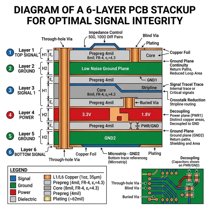
While back drilling is a highly effective remedy for stub-related signal issues, it introduces additional manufacturing steps and complexity. Because the back drill diameter must be inherently larger than the primary via hole, the anti-pad (clearance) on the reference planes the drill passes through must also be correspondingly enlarged. This alteration can heavily impact your controlled impedance routing if not carefully managed and accounted for in your impedance calculations.
Frequently Asked Questions About Back Drilling
At what frequency is back drilling absolutely necessary?
Generally speaking, back drilling becomes a crucial requirement for signals operating at data rates above 3 Gbps. However, even at lower frequencies like 1 Gbps to 2 Gbps, it can prove incredibly beneficial if your design has very tight timing margins, uses older driver technology, or if the via stubs are exceptionally long due to routing through a very thick board or backplane.
Does implementing back drilling increase PCB costs?
Yes, back drilling inherently adds to the overall manufacturing cost and potentially extends the lead time. It requires a completely secondary drilling process using specialized equipment with highly precise Z-axis depth control. It’s important to carefully weigh this added cost against the strict performance requirements of your design and selectively apply it only on the critical nets that genuinely need it.
Can I use blind or buried vias instead of back drilling?
Yes, utilizing blind and buried vias are valid alternative solutions to effectively eliminate via stubs. However, the sequential lamination process required to create blind or buried vias can sometimes be significantly more expensive and complex to manufacture than a standard multi-layer board coupled with back drilling. The optimal choice usually depends on the specific layer transitions required in your design and the overall cost constraints of the project.