When it comes to printed circuit board (PCB) manufacturing and design, ensuring the longevity and reliability of your boards is paramount. One of the most common and effective ways to protect your PCBs is through via tenting techniques. In this article, we’ll dive deep into what via tenting is, why it’s crucial for your circuit boards, and how to effectively implement it.
What is Via Tenting?
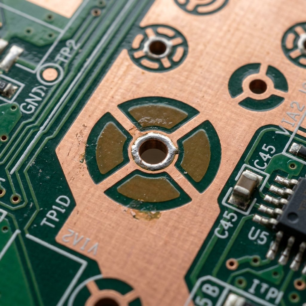
Via tenting refers to the process of covering a PCB via with a solder mask to completely enclose or “tent” the hole. Unlike exposed vias, tented vias prevent exposure to environmental factors and minimize the risk of electrical shorts. The solder mask acts as a protective layer, sealing the via and maintaining the integrity of the circuit.
To fully understand the context of via protection, it is helpful to explore Why PCB Solder Mask Clearance Matters for Defect-Free Soldering. Proper solder mask application, including clearance and tenting, is the foundation of a robust PCB.
The Benefits of Via Tenting
Implementing effective via tenting techniques offers several distinct advantages:
- Prevention of Solder Bridging: During wave soldering or surface mount assembly, exposed vias close to surface mount pads can draw solder away or cause shorts. Tenting vias prevents this bridging.
- Protection Against Oxidation: Copper inside the via barrel is prone to oxidation. Tenting seals it away from moisture and air, preserving its conductivity.
- Improved Assembly Reliability: By preventing solder wicking into vias, you ensure that the correct amount of solder remains on the component pads. This is a critical factor, similar to what you learn when applying Essential PCB Pad Design Tips for Reliable SMT Assembly.
How to Implement Via Tenting in Your PCB Design
Follow these steps to effectively tent vias in your PCB layout software.
Step 1: Identify Vias to Tent
Determine which vias require tenting. Typically, vias placed near fine-pitch components, BGA pads, or in high-density areas should be tented to prevent solder wicking and shorts.
Step 2: Adjust Solder Mask Expansion
In your PCB design software, set the solder mask expansion for the selected vias to a negative value or zero, ensuring the mask completely covers the via hole and annular ring. Keep in mind that a well-designed annular ring is essential for structural integrity; you can read more on How to Design the Perfect PCB Annular Ring to Prevent Breakouts.
Step 3: Verify Tenting in 3D Viewer or Gerber Files
Before sending your design to manufacturing, visually inspect the Gerber files or use your CAD tool’s 3D viewer to confirm that the vias are covered by the solder mask layer.
Step 4: Communicate with Your Manufacturer
Ensure your fabrication notes explicitly state the requirement for tented vias. Different manufacturers have varying capabilities regarding the maximum via size that can be reliably tented using liquid photoimageable (LPI) solder mask.
Advanced Via Protection Methods
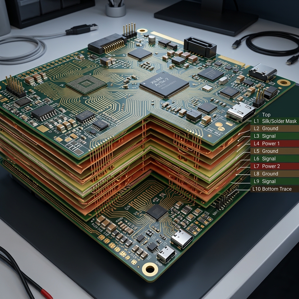
While standard LPI via tenting is suitable for most applications, high-reliability boards may require more robust solutions. These include via filling with conductive or non-conductive epoxy, followed by plating over (VIPPO). These techniques are especially common in high-density interconnect (HDI) designs where vias are placed directly in component pads. While advanced techniques add cost, they offer the highest level of protection and routing density.
When considering advanced PCB design techniques, thermal management also plays a significant role. Integrating tented vias effectively can sometimes impact heat dissipation, which is why understanding How to Optimize PCB Copper Pour for Better Thermal Dissipation is vital alongside your via strategy.
Frequently Asked Questions
What is the maximum via size that can be tented?
Typically, standard LPI solder mask can reliably tent vias with a finished hole size of up to 12 mils (0.3mm) or sometimes 15 mils. Attempting to tent larger vias may result in the mask breaking or tearing, exposing the hole.
Is via tenting always necessary?
No, it’s not strictly necessary for every board. However, it is highly recommended for dense boards, areas near surface mount pads, or when the board will be exposed to harsh environments.
What happens if a tented via breaks open during manufacturing?
If the solder mask tent breaks, it can create a trap for chemicals during the fabrication process (such as HASL fluxes). This can lead to long-term reliability issues and corrosion. This is why adhering to the manufacturer’s maximum tentable via size is critical.
Conclusion
Protecting your circuit boards with effective via tenting techniques is a relatively simple yet highly impactful step in the PCB design process. By understanding when and how to tent your vias, you can significantly reduce the risk of manufacturing defects, improve the longevity of your product, and ensure consistent electrical performance. Whether you are working on a simple two-layer board or a complex multi-layer HDI design, mastering via protection strategies is an essential skill for any electronics designer.