As printed circuit boards (PCBs) become increasingly dense and complex, ensuring reliability through robust manufacturing techniques is non-negotiable. One of the most critical aspects of modern PCB fabrication, particularly in High-Density Interconnect (HDI) boards, is via filling. This guide will cover the different via filling methods and materials to help you make informed decisions for your next PCB project.
Why Via Filling Matters
A via provides the electrical connection between different layers of a PCB. When vias are left open, they can trap contaminants, solder, and flux during assembly, leading to long-term reliability issues or short circuits. Via filling, particularly via-in-pad technology, is vital for ensuring a flat, solderable surface for components like BGAs (Ball Grid Arrays), maximizing routing space, and improving thermal and electrical performance.
Understanding these concepts is closely tied to other critical design factors. For instance, selecting the right PCB hole size for through hole components is an essential first step before determining the correct filling method.
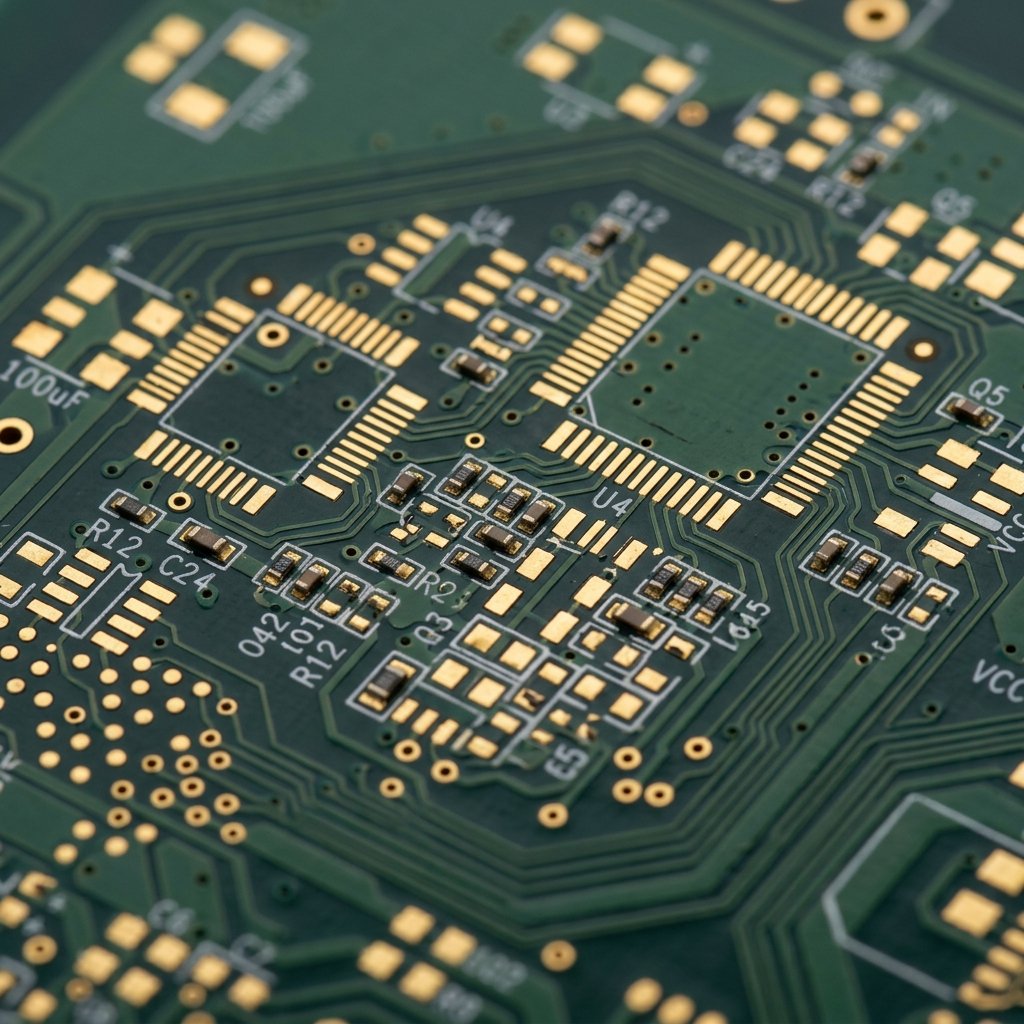
Common Via Filling Materials
Different materials serve different functional requirements, generally split between conductive and non-conductive options.
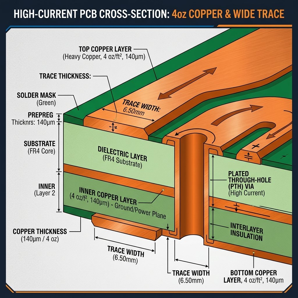
1. Non-Conductive Epoxy
Non-conductive epoxy is the most common and cost-effective via filling material. It effectively seals the via, preventing solder wicking and contamination. Although it’s non-conductive, the copper plating on the walls of the via still carries the electrical signal, making it perfectly adequate for standard HDI designs. It also expands at a rate closer to the surrounding laminate compared to conductive pastes, reducing the risk of via barrel cracking during thermal cycling.
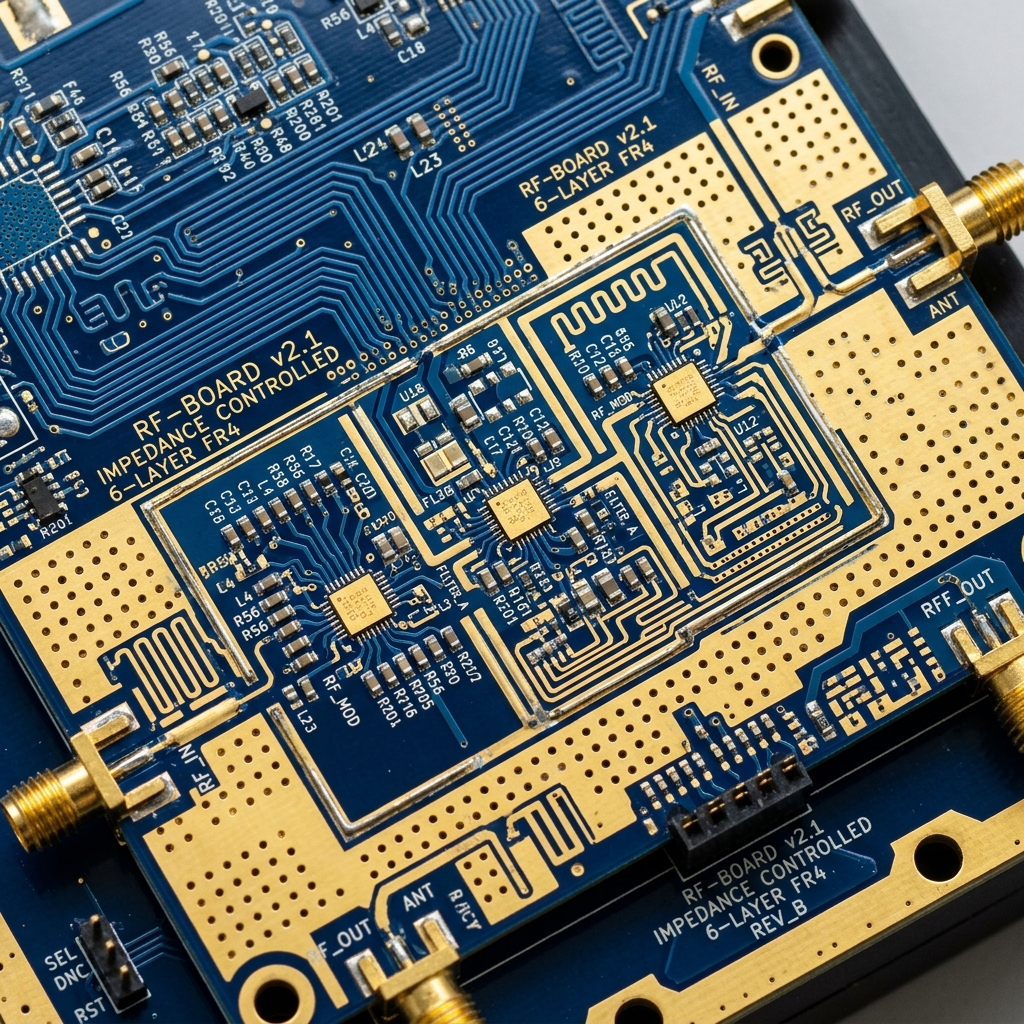
2. Conductive Paste (Silver or Copper)
Conductive pastes, filled with silver or copper particles, are used when maximum thermal and electrical conductivity is required. They are typically used to transfer large amounts of heat away from components. This goes hand in hand with how to optimize PCB copper pour for better thermal dissipation.
3. Copper Plating (Solid Copper Fill)
For microvias in HDI designs, the gold standard is solid copper plating. Instead of filling the via with an epoxy or paste, the via is continuously electroplated until it is completely filled with solid copper. This provides the ultimate electrical and thermal performance, but it is limited to small microvias and is more expensive.
How to Specify Via Filling in Your PCB Fabrication Notes
Properly documenting your via filling requirements ensures your manufacturer builds the board exactly as intended.
Step 1: Identify Vias to be Filled
Clearly designate in your Gerber files or drill files which specific vias require filling. Usually, this is done by placing them on a separate drill layer.
Step 2: Specify the Material Type
State explicitly whether you require conductive (e.g., silver/copper epoxy, solid copper) or non-conductive epoxy fill in your fabrication notes.
Step 3: Call Out IPC Standards
Reference standard IPC-4761, which categorizes different via protection types. For a fully filled and capped via-in-pad, you would typically specify IPC-4761 Type VII.
Design Considerations
When designing boards with filled vias, especially for high-density components, you must balance mechanical stability and electrical clearance. For example, maintaining a robust structure involves understanding how to design the perfect PCB annular ring to prevent breakouts. If your design involves high power, you also need to incorporate high voltage PCB clearance rules every designer must follow.
Frequently Asked Questions
What is IPC-4761 Type VII?
IPC-4761 Type VII refers to a via that is completely filled with material (usually epoxy) and then plated over with copper to create a flat, solderable pad. It is the standard requirement for via-in-pad technology.
Why not use conductive epoxy for everything?
Conductive epoxy is expensive and has a different Coefficient of Thermal Expansion (CTE) than the surrounding FR4 material. This mismatch can cause stress and cracking during temperature changes. Non-conductive epoxy is generally preferred unless extreme thermal transfer is needed.
Can I put a via in a surface mount pad without filling it?
No, this is highly discouraged. An open via in a pad will draw solder away from the component lead during reflow (solder wicking), leading to poor or missing solder joints.
In conclusion, mastering via filling techniques allows you to design smaller, more efficient, and highly reliable PCBs. By understanding the materials and correctly specifying your requirements, you can ensure a smooth manufacturing process.