Once the PCB pattern has been transferred onto the copper surface, the next step is to remove the unwanted copper.
This stage is known as PCB etching.
Although it is only one step in the manufacturing process, etching has a direct influence on trace accuracy, spacing, impedance control, and overall production quality. Even small variations during etching can affect the dimensions of fine traces and reduce manufacturing yield.
Understanding how etching works helps engineers design boards that are easier to manufacture and more consistent in production.
What Is PCB Etching?
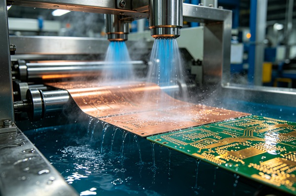
PCB etching is the process of removing exposed copper from a copper-clad laminate while protecting the required circuit pattern with a resist layer.
After etching is complete, only the copper needed for the electrical circuit remains.
The quality of this step determines whether trace widths and spacing match the original PCB design.
Before etching begins, the board already consists of a copper foil bonded to a laminate. If you’d like to understand these materials first, see PCB Copper Foil Types and Their Applications and PCB Laminate Explained for PCB Design and Manufacturing.
How the PCB Etching Process Works
Although manufacturing lines vary, the basic process follows the same sequence.
Surface Preparation
The copper surface is cleaned to remove oxidation, dust, and contaminants so the photoresist can adhere evenly.
Pattern Transfer
A photoresist is applied and exposed to ultraviolet light through the PCB artwork.
After development, the areas that will become circuit traces remain protected.
Copper Etching
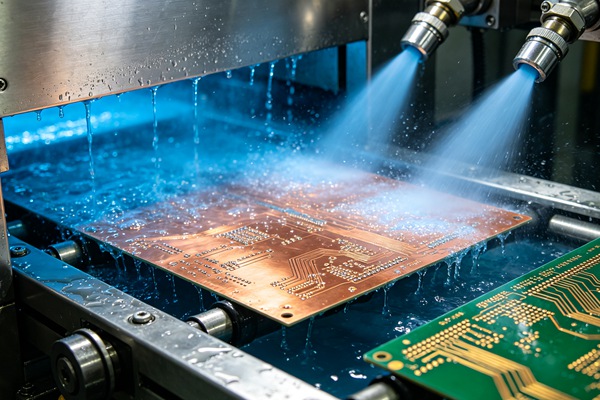
The board passes through an etching solution that dissolves the exposed copper.
The protected copper remains in place and forms the finished circuit pattern.
Resist Removal
Once etching is complete, the remaining photoresist is stripped away, leaving clean copper traces ready for the next manufacturing step.
Common PCB Etching Methods
Different production lines use different chemical systems depending on capacity and product requirements.
Ferric Chloride
Ferric chloride is widely used for prototype production and laboratory applications because it is easy to handle and provides stable results.
Cupric Chloride
Cupric chloride is common in high-volume manufacturing because the solution can be regenerated and controlled during continuous production.
Alkaline Etching
Alkaline etching is widely used for fine-line PCB production and offers good control over trace dimensions.
The specific chemistry varies between manufacturers, but the goal remains the same: remove only the unwanted copper while preserving the designed circuit pattern.
Why Etching Accuracy Matters
Etching affects more than the appearance of the PCB.
Trace Width
Over-etching can make traces narrower than intended, while under-etching may leave unwanted copper behind.
Trace Spacing
Accurate etching helps maintain the required clearance between adjacent conductors.
This becomes increasingly important for high-density layouts.
Signal Integrity
Controlled trace geometry contributes to stable impedance and predictable electrical performance.
For designs with controlled impedance, material selection also plays an important role. FR4 PCB Stackup Design Guide explains how stackup and dielectric thickness work together with trace dimensions.
Manufacturing Yield
Stable etching processes reduce defects and improve production consistency, especially for multilayer and fine-pitch boards.
Factors That Influence Etching Quality
Several variables affect the final result.
These include:
- Copper thickness
- Trace width
- Etchant concentration
- Solution temperature
- Spray pressure
- Conveyor speed
- Photoresist quality
Maintaining these parameters within specification helps achieve consistent production.
Common Etching Defects
Manufacturers monitor the process closely to reduce defects.
Typical issues include:
- Over-etching
- Under-etching
- Uneven trace width
- Copper residue
- Edge roughness
Modern production lines use automated process control to minimize these problems.
How to Improve PCB Etching Quality
- Step 1
Use trace widths and spacing that match the manufacturer’s capabilities.
- Step 2
Select an appropriate copper thickness during the design stage.
- Step 3
Ensure the photoresist pattern is accurately transferred before etching.
- Step 4
Work with a PCB manufacturer that maintains stable process control throughout production.
Conclusion
PCB etching is one of the most critical stages in circuit board fabrication.
By removing unwanted copper while preserving the designed circuit pattern, the process determines the accuracy of traces, spacing, and overall manufacturing quality.
Careful process control, combined with appropriate PCB design rules, helps produce reliable boards that meet both electrical and mechanical requirements.
Frequently Asked Questions
A: PCB etching is the process of removing unwanted copper from a copper-clad laminate to form the required circuit pattern.
A: Common etchants include ferric chloride, cupric chloride, and alkaline etching solutions, depending on the manufacturing process.
A: Etching determines trace width, spacing, and circuit accuracy, all of which influence PCB quality and electrical performance.
A: Over-etching removes too much copper, making traces narrower than designed and potentially affecting circuit reliability.
A: Yes. Thicker copper generally requires longer etching times and tighter process control to maintain accurate trace dimensions.